
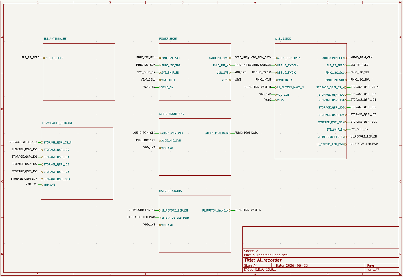
Quick Answer
Before using an AI-generated KiCad schematic for PCB layout, do not start by placing parts. First check that the schematic is electrically coherent, that every symbol has the right footprint, that the BOM maps to real orderable parts, and that the layout-critical assumptions are visible. The schematic should also define power rails, net names, connectors, keepouts, debug access, antenna constraints, thermal risks, and any DNP or tuning parts.
Treat the generated schematic as a reviewable first draft, not a layout-ready release. A good AI schematic can save time by giving you structure, sheets, nets, and component context. The PCB layout step still needs a human engineer to validate footprints, pin mapping, manufacturability, sourcing, and physical constraints before routing.
Why This Matters
An AI-generated schematic can look complete while still being risky for layout. The most common failure is not that the drawing is empty. The harder problem is that the schematic may hide layout assumptions: the wrong package variant, a missing programming header, unclear connector orientation, no antenna keepout, weak power sequencing, or BOM parts that cannot actually be sourced.
PCB layout turns abstract nets into physical copper, mechanical placement, thermal behavior, signal integrity, and manufacturing files. Once a board is routed, schematic mistakes become expensive. That is why the right gate is simple: before layout starts, the KiCad project should be clear enough that a PCB designer can place parts, assign rules, route priority nets, and ask focused questions.
Have a product brief that needs an editable starting point?
Describe the architecture, power, interfaces, footprints, sourcing constraints, operating states, and expected KiCad handoff. Create a free account to start a reviewable, editable KiCad first draft.
Core PCB Layout Readiness Checklist
| Review area | What to check before layout | Why it matters for PCB layout |
|---|---|---|
| Product requirement | Confirm the schematic still matches the product goal, power source, enclosure, connectors, wireless needs, and user interactions. | Layout decisions depend on the real product, not only the electrical blocks. |
| Sheet hierarchy | Check that power, MCU, sensors, storage, RF, connectors, and UI are separated into reviewable sheets. | A clear hierarchy helps the PCB designer trace nets and spot missing interfaces. |
| Footprint assignment | Verify each symbol has the correct KiCad footprint, package variant, pin count, pad pitch, polarity, and land pattern. | Wrong footprints can make a board impossible to assemble even if the schematic looks correct. |
| Pin mapping | Compare MCU pins, connector pins, sensor buses, boot pins, reset pins, and alternate functions against datasheets. | PCB layout cannot fix swapped pins that break boot, debug, power control, or firmware assumptions. |
| Power rails | Check rail names, voltage levels, current estimates, regulator stability, decoupling, sequencing, and power-good behavior. | Power placement, plane strategy, copper width, and thermal behavior all start here. |
| Inductive loads | For switched relays, solenoids, and brushed motors, use the flyback diode schematic guide to confirm the clamp path, polarity, current path, voltage rating, and release-time requirements. | The clamp belongs close to the switching loop; choosing it after placement can increase EMI, voltage stress, and rework risk. |
| Net classes | Mark high-current, RF, USB, differential, clock, analog, battery, and sensitive sensor nets. | The PCB designer needs clear routing priorities and constraint groups before placement. |
| Connectors | Confirm connector type, pin numbering, orientation, mating direction, mounting holes, cable access, and mechanical clearance. | Connector mistakes often survive schematic review but fail in enclosure or assembly. |
| RF and antenna | Check antenna part, matching network, keepout, ground clearance, nearby metal, enclosure notes, and tuning placeholders. | RF layout depends on physical geometry, not schematic connectivity alone. |
| BOM and sourcing | Confirm MPNs, lifecycle, stock, substitutions, quantity, package, tolerance, voltage rating, and DNP/tuning status. | A PCB layout based on unavailable or wrong-package parts can force a redesign. |
| Manufacturing handoff | Confirm design rules, board outline, mounting holes, test points, fiducials, silkscreen notes, and assembly constraints. | These details determine whether the design can move from schematic to fab and assembly smoothly. |
Footprint Checks That Deserve Extra Attention
Footprints are the first place to slow down. In a generated KiCad project, a symbol may be electrically plausible while the physical footprint is still wrong. Before layout, check the manufacturer package drawing against the assigned KiCad footprint, especially for USB-C connectors, QFN/QFP packages, MEMS microphones, chip antennas, PMICs, battery connectors, and small sensors.
The nRF54L15 development-board KiCad project is a concrete example: its generated target sheet uses a provisional nRF52832 surrogate, so the exact nRF54L15 symbol, package-specific pinout, footprint, reference circuit, and layout must be replaced or verified together before placement.
For every layout-critical part, confirm pad pitch, exposed pad size, pin numbering, courtyard, solder mask expansion, assembly orientation, and 3D/mechanical fit if available. If the project uses local symbols or local footprints, review those files directly instead of assuming the library name is enough.
BOM Checks Before Placement
A BOM review is not just a purchasing task. It tells the PCB designer whether the schematic is tied to real parts with real packages. Before placement starts, check that every important component has a manufacturer part number, package, electrical rating, availability, and a sensible alternate strategy.
Pay special attention to passives around power, RF, USB, oscillators, sensors, and analog front ends. A generated schematic may include reasonable resistor or capacitor values, but the BOM still needs voltage rating, tolerance, temperature behavior, package size, and DNP/tuning intent. For a deeper upstream review flow, use the existing AI-generated KiCad schematic review guide before moving into layout.
Example From a Real SpeedUp Project
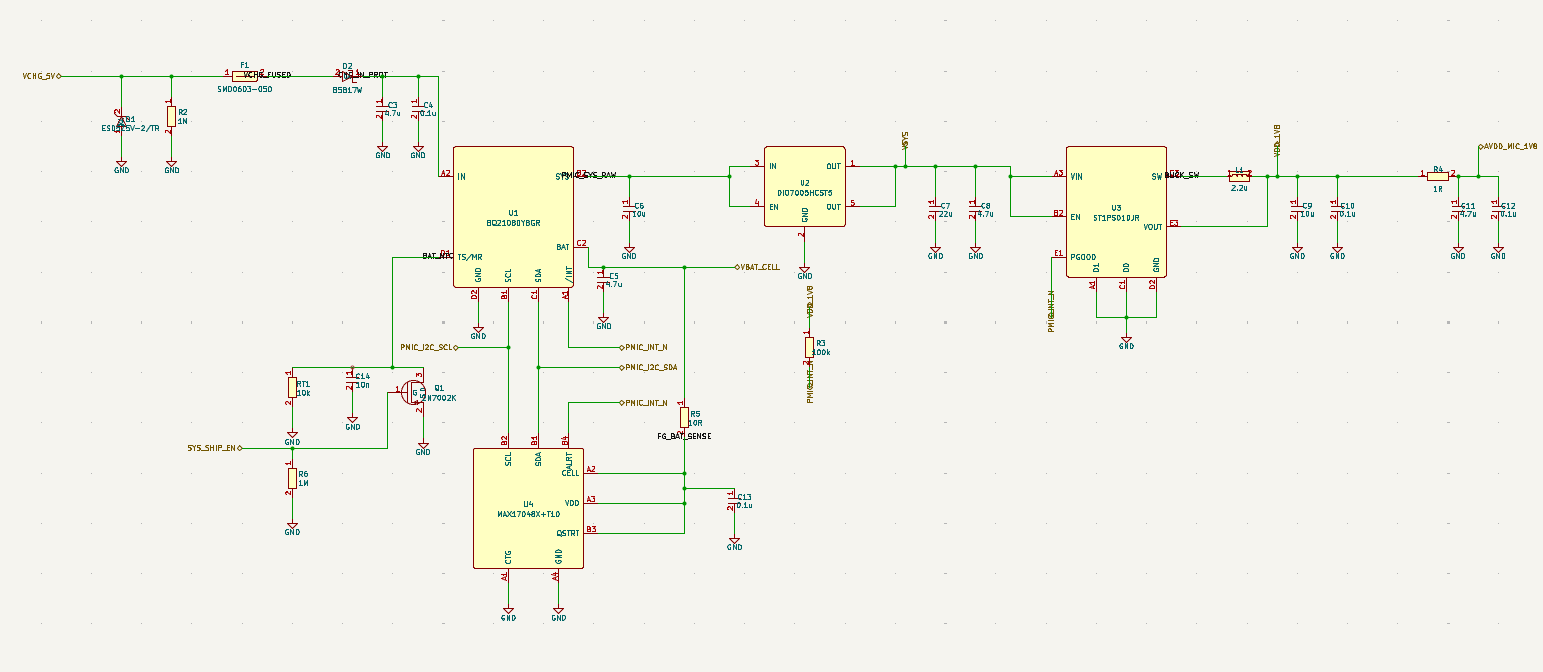
The running example here is the magnetic AI label microphone KiCad project. The prompt asked for a tiny magnetic AI label microphone that records continuously, supports real-time transcription, and syncs to a phone over BLE.
That kind of device is a useful layout-readiness test because it combines battery charging, a BLE SoC, PDM audio capture, QSPI storage, RF antenna placement, status I/O, and a small enclosure. Before layout, the schematic needs to show more than connectivity. It should help the PCB designer understand which nets are sensitive, which parts must stay close, which blocks need keepouts, and which assumptions still require engineering review.
For example, the power management sheet should lead to questions such as:
- Where should the charger, regulator, fuel gauge, battery connector, and decoupling capacitors sit?
- Which traces carry charging or load current?
- Which I2C lines need pullups and test access?
- Which rails need wider copper, thermal relief review, or extra probing points?
- Are any battery, USB, enclosure, or magnetic mounting assumptions missing?
The schematic is useful because it makes those questions concrete. It is still not enough by itself. Layout should start only after the engineer confirms that the parts, footprints, nets, and physical constraints are ready for placement.
Common Mistakes
- Starting PCB layout before footprint review is complete.
- Treating a generated BOM as valid without checking MPNs, packages, lifecycle, stock, and substitutions.
- Forgetting that connector orientation and pin numbering are physical decisions, not just schematic symbols.
- Routing RF, USB, clock, high-current, or analog nets without net-class notes and placement priorities.
- Assuming a chip antenna or MEMS microphone will work without keepout, enclosure, and vendor layout guidance.
- Skipping test points, programming access, boot strapping, and manufacturing fixtures until after routing.
- Letting DNP and tuning parts look like normal production parts in the BOM.
How SpeedUp Fits
SpeedUp is useful at the stage before manual schematic cleanup and PCB layout. You can describe the product, generate a first KiCad schematic draft, then review the sheets, BOM context, and project structure with an engineer. That gives the layout discussion a concrete starting point instead of a blank KiCad file.
The right workflow is still human-reviewed. Use SpeedUp to create a structured first pass, then validate power, footprints, BOM, layout constraints, sourcing, thermal behavior, RF guidance, firmware assumptions, and test strategy. For broader context on generated circuit drafts, read the AI schematic generator guide.
Related Guides And Project Examples
- How to review an AI-generated KiCad schematic for the upstream schematic review process.
- Temperature and humidity sensor KiCad project for a battery-powered sensor example with charging, I2C sensing, display, and BOM review points.
- Battery-powered sensor circuit design checklist when your layout handoff involves sensors, batteries, sleep current, and low-power constraints.
FAQ
Is an AI-generated KiCad schematic ready for PCB layout?
Not automatically. It may be a useful first draft, but it should pass schematic review, footprint review, BOM review, and layout-readiness checks before placement and routing begin.
What should I check first before PCB layout?
Start with footprints, pin mapping, power rails, connectors, and BOM availability. If those are wrong, the layout can become unusable even when the schematic appears complete.
Why are footprints risky in AI-generated schematics?
The schematic symbol can be electrically plausible while the footprint uses the wrong package, pad size, pin numbering, orientation, or mechanical outline. Always compare the assigned footprint against the manufacturer package drawing.
Should BOM review happen before or after PCB layout?
Do a first BOM review before layout. The PCB designer needs to know whether parts are real, orderable, correctly packaged, and stable enough to place. A deeper sourcing review can continue later, but package and availability problems should be caught early.
Can SpeedUp replace PCB layout review?
No. SpeedUp helps generate a structured schematic and KiCad starting point. Engineers still need to review footprints, layout constraints, routing, manufacturing files, test access, compliance, and production risks.
Start With a Reviewable KiCad Draft
Turn your product requirements into structured schematic sheets that can proceed into engineering review.
Use SpeedUp to turn the product requirements into structured schematic sheets and an editable KiCad first draft for engineering review. Create a free account to begin.
Comments
No comments yet.
Leave a Reply