
If you are evaluating an AI schematic generator, this project shows a concrete circuit example instead of a generic feature list. SpeedUp turned a natural-language prompt into an editable KiCad project for an all-in-one electronics debugging tool with a 12V adjustable power supply, limited DMM-style measurement, logic analyzer inputs, a PWM output, and a simple single-channel oscilloscope interface around a small display.
This is a first engineering draft for review, not a production-ready reference design. The downloadable package includes the editable KiCad 10 project, five hierarchical schematic sheets, BOM exports, local symbol and footprint libraries, and a PCB file with component placement but no routed copper segments or vias.
Project Summary
| Field | Details |
|---|---|
| Project | All-in-one debugging tool for electronics bench work |
| Input | Natural-language product prompt |
| Output | Editable KiCad 10 schematic project, BOM, local libraries, and a placed but unrouted PCB file |
| Key modules | POWER_INPUT, CONTROL_UI, ADJUSTABLE_PSU, ANALOG_FRONTEND, DIGITAL_IO |
| Included files | debug_tool.kicad_pro, top-level and five hierarchical schematic sheets, debug_tool.kicad_pcb, CSV/XLSX BOM, 15 symbol libraries, 37 footprints, and project-evidence images |
| Next engineering work | PCB placement review and routing, firmware, BOM review, mechanical enclosure, calibration plan, and bench validation |
| Status | First engineering draft for review |
The Prompt
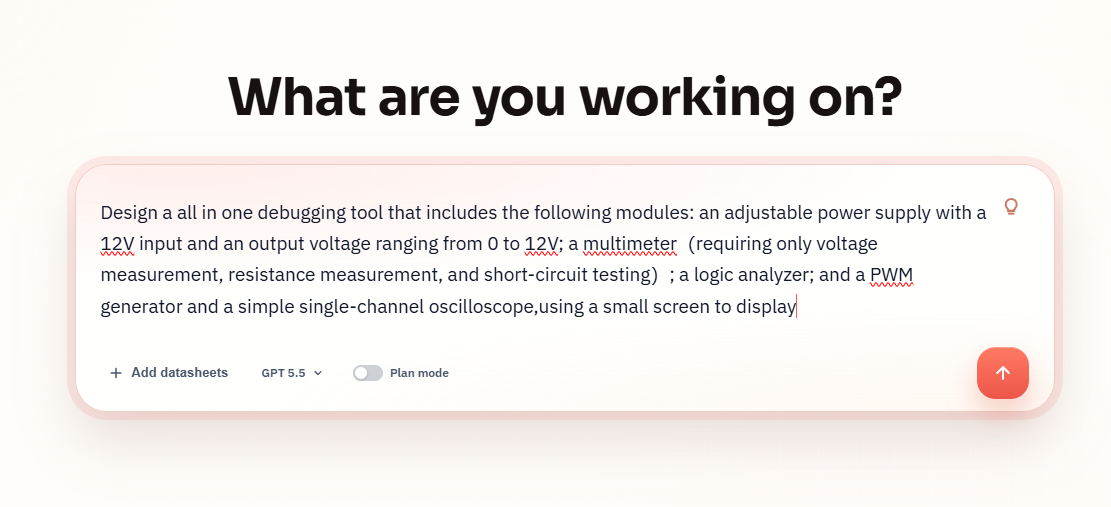
The project starts with this plain-language device request:
Design a all in one debugging tool that includes the following modules: an adjustable power supply with a 12V input and an output voltage ranging from 0 to 12V; a multimeter(requiring only voltage measurement, resistance measurement, and short-circuit testing); a logic analyzer; and a PWM generator and a simple single-channel oscilloscope,using a small screen to display
What SpeedUp Generated
SpeedUp used the prompt as an AI circuit schematic generator input and produced a structured editable KiCad project with:
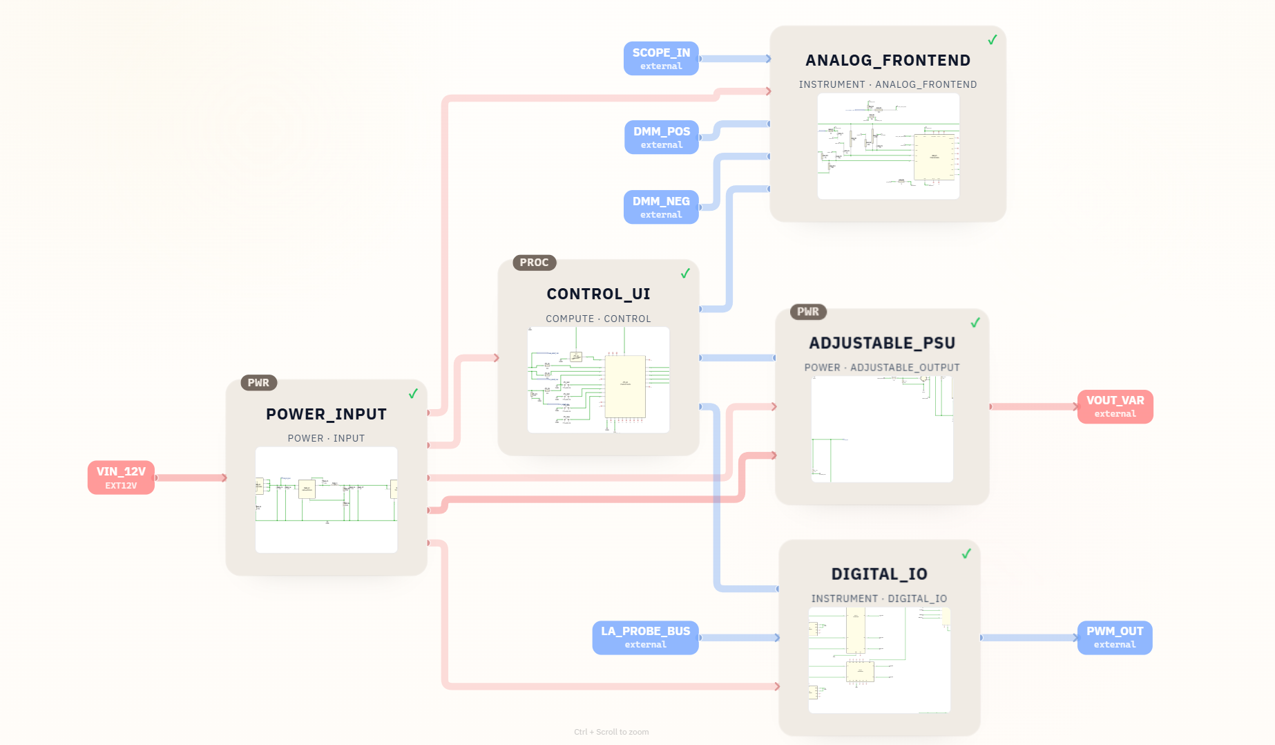
- A system block diagram for the debugging tool architecture.
- A top-level hierarchical schematic showing the main modules and named nets.
- A
POWER_INPUTpath forVIN_12V,VIN_12V_BUS, and3V3_SYS. - An
ADJUSTABLE_PSUmodule with a variable output path labeledVOUT_VAR. - An
ANALOG_FRONTENDmodule connected toSCOPE_IN,DMM_POS, andDMM_NEG. - A
DIGITAL_IOmodule connected toLA_PROBE_BUSandPWM_OUT. - Detail screenshots for the PSU, analog front end, and digital I/O / PWM circuitry.
- A downloadable source package containing
debug_tool.kicad_pro,debug_tool.kicad_sch, five module sheets,debug_tool.kicad_pcb, BOM exports, local libraries, and project-evidence images.
The result is useful as an engineering starting point because it is not just a text concept or screenshot set. Engineers can open debug_tool.kicad_pro in KiCad 10, inspect the named modules and nets, edit the schematic source, review the BOM, and continue the placed but unrouted PCB file.
Want to create a multi-function debugging tool?
Describe your own multi-function electronics debugging tool requirements and create a free account to start a reviewable engineering draft.
Project Architecture
The featured block diagram organizes the design into five reviewable modules:
POWER_INPUT: accepts the external 12V input and distributes power rails into the rest of the design.CONTROL_UI: acts as the central compute and control block, linking the power supply, analog measurement path, digital I/O path, and display/UI behavior.ADJUSTABLE_PSU: converts the 12V input path into a variable external output labeledVOUT_VAR.ANALOG_FRONTEND: handles oscilloscope and simplified multimeter input paths throughSCOPE_IN,DMM_POS, andDMM_NEG.DIGITAL_IO: groups the logic analyzer probe bus and PWM output path around the digital interface circuitry.
That architecture matches the original prompt closely: power generation, measurement, logic analysis, PWM generation, and single-channel scope capture are separated into modules instead of being flattened into one unreadable sheet.
AI Schematic Generator Output
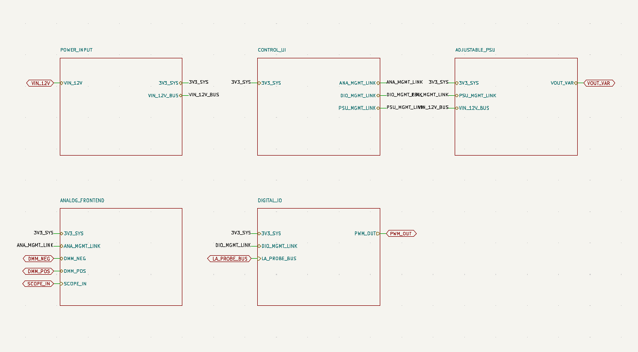
The top-level sheet is the main proof that the generated output has an engineering structure. It includes external ports such as VIN_12V, VOUT_VAR, SCOPE_IN, DMM_POS, DMM_NEG, LA_PROBE_BUS, and PWM_OUT, which makes the project easier to review than a single flat concept diagram.
The source package contains the top-level debug_tool.kicad_sch plus POWER_INPUT, ADJUSTABLE_PSU, ANALOG_FRONTEND, DIGITAL_IO, and CONTROL_UI sheets. It also includes 15 local symbol libraries and 37 local footprint files so the generated project remains editable as an engineering handoff.
Bench Power Supply and Adjustable Power Supply Schematic Detail
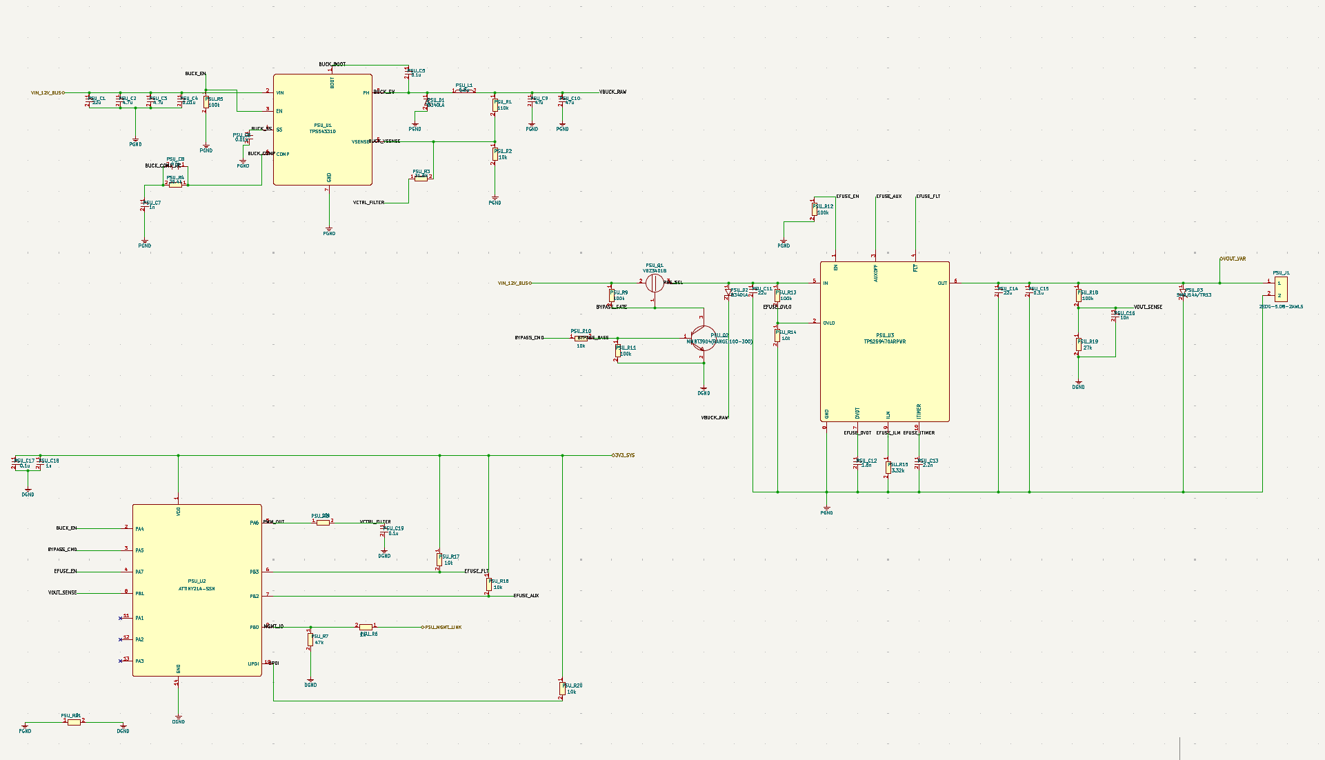
The adjustable power supply is one of the most important subsystems because it touches both usability and safety. As a bench power supply schematic example, the generated sheet shows a VIN_12V_BUS input path, a buck-style conversion stage, control signals, filtering, a protected output path, and a VOUT_VAR connector.
Before this subsystem can become hardware, engineers should review:
- Whether the selected regulator and protection devices support the requested 0 to 12V output behavior.
- Output current limits, thermal behavior, and short-circuit response.
- Control-loop stability across load, cable, and output-capacitance conditions.
- Output voltage sensing accuracy and firmware behavior during startup and fault recovery.
- Connector rating, reverse-polarity handling, and safe user access to the external output.
For a bench tool, this section deserves extra caution. A variable supply that shares enclosure space with measurement inputs can create awkward ground, protection, and user-error cases if the product architecture is not reviewed as a whole.
Analog Front End Detail
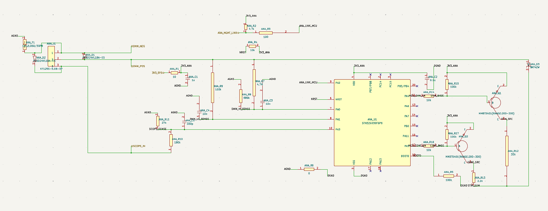
The analog front end carries the simplified multimeter and single-channel oscilloscope intent from the prompt. The generated sheet includes DMM_POS, DMM_NEG, SCOPE_IN, analog management links, input protection, resistor networks, and a microcontroller-side measurement path.
This is where the project needs careful review before anyone treats it as a measurement instrument. Key questions include:
- What voltage range is safe at
SCOPE_IN,DMM_POS, andDMM_NEG? - Is the oscilloscope path buffered, attenuated, and bandwidth-limited correctly?
- Can the resistance and short-circuit test modes avoid back-driving an external circuit?
- Are analog ground, digital ground, and user-accessible connector references handled safely?
- What calibration process is required before readings are trustworthy?
The generated schematic is a useful first draft because it separates the analog measurement path from the digital I/O block. It still needs real component validation, tolerance analysis, noise testing, and calibration planning.
Logic Analyzer Circuit and PWM Generator Circuit Detail
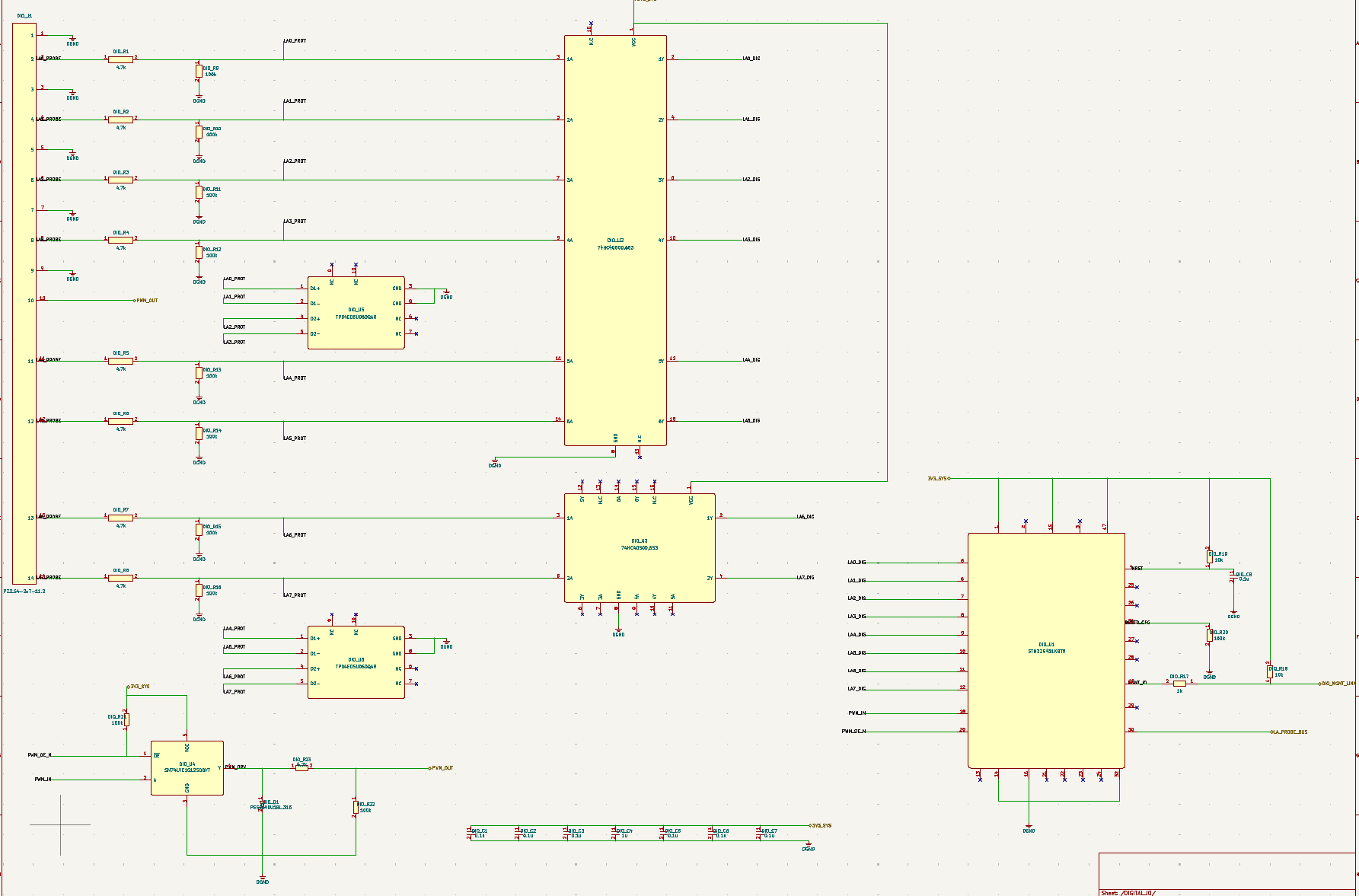
The digital section supports two requested functions: a logic analyzer circuit and a PWM generator circuit. In the generated detail, the LA_PROBE_BUS routes through the digital I/O circuitry, while PWM_OUT is exposed as an external output.
For this subsystem, the most important review topics are input protection and timing behavior:
- Logic analyzer input thresholds must match the target voltage families the tool claims to support.
- Probe loading should be low enough that the debugging tool does not disturb the circuit under test.
- ESD and overvoltage events need a defined protection strategy.
- Sampling rate, trigger logic, memory depth, and display refresh are firmware and hardware co-design problems.
- PWM output amplitude, drive strength, rise time, duty-cycle range, and frequency range need explicit specifications.
The schematic screenshot shows the right kind of review surface: named nets, buffering/protection devices, and a clear distinction between input capture and PWM output. The bundle does not yet prove firmware behavior, protocol decoding, timing accuracy, or UI quality.
BOM Preview
The included BOM contains 71 line items and 159 placed quantities. Its reference totals match the 159 footprints in debug_tool.kicad_pcb, providing a concrete starting point for component, footprint, sourcing, and layout review.
The BOM covers power conversion ICs, protection devices, microcontroller and control devices, input-conditioning resistors, capacitors, connectors, and digital buffer/protection parts. Engineers should still review availability, alternates, footprint accuracy, package ratings, cost, tolerances, and assembly constraints before release.
For this project, a complete BOM should also separate measurement-critical parts from general support parts. Resistor tolerances, ADC reference behavior, input protection leakage, connector ratings, and regulator thermal performance will matter more than they would in a simple LED or sensor board.
What Still Needs Human Review
This generated project is a first engineering draft. Before layout, firmware, or manufacturing, the design should be reviewed for:
- Electrical safety around the external 12V input and variable output.
- Short-circuit behavior in both the adjustable power supply and DMM test modes.
- Analog input protection for oscilloscope and multimeter use.
- Logic analyzer threshold support, ESD protection, and probe loading.
- PWM output voltage level, current capability, frequency range, and edge behavior.
- Grounding between power, analog measurement, digital I/O, and display/control sections.
- Thermal performance of power conversion and protection devices.
- Calibration requirements for voltage measurement, resistance measurement, and oscilloscope display.
- Firmware responsibilities for UI, measurement modes, capture timing, protection states, and error handling.
- PCB placement and routing, enclosure design, connector placement, labeling, BOM verification, and test procedure.
The strongest use of this bundle is as a starting point for design review. It lets a hardware engineer see how SpeedUp decomposed the prompt into subsystems, then decide what needs replacement, validation, or expansion.
Related SpeedUp Projects and Guides
- Read the AI schematic generator for KiCad circuit projects guide for the broader prompt-to-schematic workflow behind this debugging tool circuit.
- Use the schematic review checklist for AI-generated KiCad projects before turning generated instrument circuits into PCB layout work.
- Compare this tool-style build with the desktop robot ESP32 KiCad schematic project for another generated multi-subsystem hardware example.
FAQ
Is this design production ready?
No. This is a first engineering draft for review, not a production-ready reference design. It still needs PCB layout, firmware, BOM review, safety review, calibration, and bench validation before it can be treated as a hardware product.
Why is this an AI schematic generator example?
The article shows the full prompt-to-schematic path: a natural-language request, a generated architecture diagram, a top-level schematic screenshot, and subsystem detail images for power, analog measurement, logic analysis, and PWM output. That makes it useful for evaluating what an AI schematic generator can produce as a first reviewable draft.
What files are included in the generated bundle?
The ZIP includes debug_tool.kicad_pro, debug_tool.kicad_sch, five hierarchical schematic sheets, debug_tool.kicad_pcb, CSV/XLSX BOM files, 15 symbol libraries, 37 footprint files, and prompt, block-diagram, and top-level-schematic images.
Can this project be opened directly in KiCad?
Yes. Open debug_tool/debug_tool.kicad_pro in KiCad 10. The source package includes the local symbol and footprint tables; the PCB file has 159 placed footprints but no routed copper segments or vias, so routing and layout validation remain downstream work.
What should engineers review first?
Start with the power path and analog input protection. The adjustable supply, DMM inputs, and oscilloscope input all touch external user connections, so their ratings, protection strategy, grounding, and failure behavior should be reviewed before any PCB work.
Can I generate a similar project from my own prompt?
Yes. SpeedUp is designed to turn a natural-language hardware idea into structured engineering artifacts that can be reviewed and refined. For better downstream output, include target voltage ranges, current limits, bandwidth goals, logic voltage levels, display size, enclosure constraints, and whether you need editable KiCad files, PCB layout, firmware, and BOM exports.
Download the Editable KiCad Project
Use this ZIP as a review starting point for the generated all-in-one debugging tool KiCad project. It includes the editable project and schematic source, five module sheets, a placed but unrouted PCB file, BOM exports, local symbol and footprint libraries, and prompt, architecture, and top-level schematic images.
Before treating it as a complete engineering handoff, complete and validate PCB placement and routing, review the BOM and footprints, add firmware and enclosure files, define calibration and test procedures, run bench and safety validation, and prepare manufacturing documentation.
Create Your Own Electronics Debugging Tool
Turn your own multi-function electronics debugging tool brief into reviewable engineering artifacts.
Use SpeedUp to generate structured schematic sheets and an editable KiCad project for engineering review. Create a free account to begin.
Comments
No comments yet.
Leave a Reply