
Quick Answer
A buck converter circuit is a switching DC-DC power supply that produces a regulated output voltage lower than its input voltage. A complete circuit normally includes a buck-regulator IC or controller, switching devices, an inductor, input and output capacitors, feedback or digital voltage-setting connections, enable logic, grounding, and any required protection. In an ideal continuous-conduction model, duty cycle is approximately D = VOUT / VIN, but real component values and operating limits must come from the selected IC’s data sheet and be checked across the full input, load, temperature, and transient range.
Start with requirements—not a copied reference schematic. Define VIN(min), VIN(max), VOUT, maximum and minimum load, allowed ripple, startup behavior, efficiency, thermal limits, and fault conditions. Then select a regulator and use its documented equations, recommended external components, simulation model, and evaluation-board layout as the design basis. The schematic is only the first engineering artifact: PCB layout, thermal behavior, control-loop stability, EMI, sourcing, safety, and bench performance still need human validation.
Why Buck Converter Circuit Design Matters
A buck converter can be efficient and compact, but it is not simply a voltage-regulator symbol with an inductor attached. The input capacitor carries pulsed current, the switch node has fast voltage edges, the inductor must tolerate peak current without saturating, and the output network participates in ripple and transient behavior. A schematic that ignores one of those relationships can look complete while still producing excessive ripple, unstable startup, overheating, ringing, radiated noise, or unreliable operation at the ends of the input and load range.
The first design decision is whether a buck topology is even appropriate. It is suitable when the required output remains below the available input under all supported conditions. If the input can fall below the required output, a pure buck stage cannot regulate upward; the system may need a buck-boost topology, a different rail architecture, or an explicitly accepted dropout interval.
Define the Power Requirements Before Drawing the Schematic
| Requirement | What to define | Why it changes the buck converter circuit |
|---|---|---|
| Input range | Minimum, nominal, maximum, startup ramp, surge, and source impedance | Sets IC voltage rating, duty-cycle range, current stress, protection, and dropout behavior |
| Output rail | Nominal voltage, tolerance, ripple limit, and sequencing | Determines fixed versus adjustable output, feedback design, capacitor targets, and supervisor logic |
| Load | Maximum current, minimum current, sleep current, and transient step | Drives switch rating, inductor current, operating mode, transient response, and thermal loss |
| Efficiency | Priority at full load, light load, or both | Affects topology, switching frequency, quiescent current, synchronous rectification, and mode selection |
| Environment | Ambient range, cooling, enclosure, altitude, and nearby heat sources | Changes derating, copper area, component temperature, and achievable continuous current |
| Faults | Short circuit, reverse current, hot plug, overvoltage, and misconnection | Determines whether internal protection is enough or external limiting and isolation are required |
| Noise constraints | Sensitive analog, RF, audio, sensor, or clock circuits on the same board | Influences frequency choice, filtering, rail partitioning, switching-node placement, and test plan |
| Control behavior | Enable default, power-good use, shutdown state, and firmware dependency | Prevents floating pins, unsafe startup states, and undocumented sequencing assumptions |
This requirement-first approach fits the broader electronic circuit design workflow: define the electrical job, choose an architecture, then capture the decisions in a structured schematic rather than letting a convenient part number define the product.
How a Buck Converter Circuit Works
A buck converter alternates the switch node between the input supply and a lower potential. When the high-side switch is on, current through the inductor rises and energy is delivered to the load. When it turns off, inductor current continues through either a diode in an asynchronous design or a controlled low-side MOSFET in a synchronous design. The output capacitor absorbs the difference between inductor current and load current, reducing the switching ripple seen by the load.
For an ideal converter in continuous conduction, the average output is approximately:
VOUT ≈ D × VIN
So an ideal 5 V to 3.3 V conversion implies a duty cycle near 0.66. That is a useful mental model, not a complete design calculation. Switch resistance, diode or MOSFET loss, control architecture, minimum on/off time, operating mode, current limit, and input/output ripple all move the real operating point. The Analog Devices explanation of step-down regulators shows the two switching phases and why the inductor current rises and falls.
What Belongs in a Buck Converter Schematic?
| Schematic block | What a reviewer should see | Common failure if it is wrong or missing |
|---|---|---|
| Regulator IC or controller | Exact orderable part, package, voltage/current limits, operating mode, exposed-pad connection, and data-sheet revision | Wrong variant, unsupported input range, insufficient current, or incorrect package |
| Input network | Bulk and high-frequency capacitors, voltage rating, effective capacitance, source protection, and local return | Input droop, ringing, hot-plug stress, or high pulsed-current loop inductance |
| Switching path | Integrated or external switches, diode if asynchronous, bootstrap parts when required, and clearly named SW node | Excess switch stress, shoot-through risk, or an uncontrolled high-frequency current path |
| Inductor | Inductance, tolerance, saturation current, RMS current, DCR, package, and sourcing option | Saturation, overheating, excessive ripple, or poor transient behavior |
| Output network | Capacitance, ESR assumptions, voltage rating, DC-bias derating, and load connection | Ripple, instability, slow recovery, or unacceptable overshoot and undershoot |
| Feedback or voltage selection | Divider values or digital strap states, reference source, optional feed-forward capacitor, and quiet return | Wrong output voltage, noise injection, or an undocumented power state |
| Enable and power-good | Defined default state, thresholds, pull-up voltage, timing, and firmware ownership | Floating enable, false power-good, startup races, or a rail that cannot be shut down safely |
| Ground and test access | Power-ground intent, quiet feedback ground, input/output test points, and measurement notes | Ambiguous return currents and measurements that hide switching ripple or ground bounce |
Designing a product around a buck converter?
Describe the input range, output rail, load transients, switching target, thermal limits, and protection requirements. Create a free account to start a reviewable, editable KiCad first draft.
Choose the Buck Converter IC
Begin with electrical limits. The IC’s absolute maximum rating is not the intended operating point, so choose an operating input range that includes tolerance, adapter variation, battery state, hot-plug behavior, and expected transients with suitable margin. Check the guaranteed output-current capability at the actual input, output, switching frequency, and thermal conditions; a headline current rating does not prove that a small board inside a sealed enclosure can deliver that current continuously.
Then compare control and integration choices:
- Synchronous versus asynchronous: a synchronous converter replaces the catch diode with a controlled MOSFET, often reducing conduction loss, but the IC controls more switching behavior.
- Fixed versus adjustable output: a fixed-output device removes the external feedback-divider tolerance and noise path; an adjustable device supports more rail values but requires a carefully routed divider.
- Forced PWM versus power-save mode: forced PWM can make the switching spectrum more predictable, while pulse-skipping or burst modes may improve light-load efficiency. The tradeoff matters for RF, audio, and precision analog loads.
- Internal versus external compensation: internally compensated devices simplify the schematic but impose documented ranges for inductance and output capacitance. External compensation offers flexibility but requires loop design and validation.
- Quiescent current and shutdown current: these can dominate battery life when the product sleeps most of the time.
- Minimum on-time, maximum duty cycle, and dropout: these determine whether the requested rail can be maintained at both high and low input voltage.
Also review current limit, short-circuit response, thermal shutdown, soft start, reverse-current behavior, discharge behavior, switching-frequency tolerance, package assembly, availability, and vendor design tools. Do not substitute a nominally similar part without repeating the component and loop checks.
Calculate and Select the Inductor
In continuous-conduction mode, an initial estimate of peak-to-peak inductor ripple current is:
ΔIL ≈ ((VIN − VOUT) × D) / (L × fSW)
Rearranging gives an initial inductance target:
L ≈ ((VIN − VOUT) × D) / (fSW × ΔIL)
The calculation must be evaluated at the relevant input-voltage and frequency corners, then reconciled with the regulator data sheet’s allowed inductance range. Texas Instruments’ buck power-stage calculation guide uses 20% to 40% of maximum output current as one starting estimate for ripple current, but that range is a design heuristic—not a universal requirement.
Estimate peak current as IL(peak) ≈ IOUT(max) + ΔIL / 2. The inductor saturation-current rating must remain above the actual peak and fault behavior with appropriate temperature and tolerance margin. Also check RMS current, copper DCR, core loss at the switching frequency, inductance change with bias, package height, magnetic-field sensitivity, and supplier availability. A larger inductance reduces ripple but can increase DCR, size, cost, and transient-response constraints; the best value is part of the regulator’s complete power-stage design.
Select the Input and Output Capacitors
The input capacitor supplies the converter’s pulsed switching current locally. Record more than its printed capacitance: voltage rating, dielectric, package, ESR, ESL, ripple-current capability, temperature range, and effective capacitance after DC-bias derating all matter. Include both the data-sheet minimum local capacitor and any bulk capacitance required by source impedance or cable length. The high-frequency capacitor must be placed at the power pins during PCB layout; a correct value drawn far from the IC does not create a low-inductance current loop.
The output capacitor works with the inductor and control loop. A first-order capacitive ripple estimate in continuous conduction is ΔVOUT(cap) ≈ ΔIL / (8 × fSW × COUT), with an additional ESR term approximately ΔVOUT(ESR) ≈ ΔIL × ESR. Load-transient requirements can demand more capacitance than steady-state ripple does. For internally compensated converters, remain within the vendor’s documented inductor and effective-output-capacitance range rather than increasing capacitance blindly.
Use the decoupling-capacitor value and placement guide to review dielectric, voltage coefficient, return paths, and high-frequency placement. Then confirm the selected capacitors against the regulator data sheet and the real source/load transient conditions.
Design Feedback, Enable, and Power-Good Connections
For a typical adjustable regulator, the output relation is VOUT = VFB × (1 + RTOP / RBOTTOM). Use the exact equation and bias-current guidance from the selected part. Divider resistance trades standing loss against susceptibility to feedback-pin bias, leakage, contamination, and coupled noise. Show the output-sense point explicitly, keep the feedback path away from the switch node and inductor, and return the lower divider resistor to the quiet ground location recommended by the vendor.
Some devices use fixed outputs, resistor straps, or digital inputs instead of an analog divider. In every case, document the default assembled state. An enable pin needs a defined startup level and voltage-compatible drive. A power-good pin may be open-drain and require a pull-up to an appropriate rail; its valid state while the regulator is disabled or unpowered must be understood before firmware depends on it.
Plan PCB Layout and Bench Validation From the Schematic
The schematic should carry layout intent forward. Keep the input-capacitor and switching-device current loop compact, minimize switch-node copper to what the thermal and current requirements need, place the inductor and output capacitor close to the regulator, and isolate feedback and compensation traces from the noisy switch node. Analog Devices’ step-down regulator layout guidance explains why high-di/dt loops, high-current paths, and low-level feedback paths need different routing treatment.
Add test points for input voltage, output voltage, ground, enable, and power-good. A switch-node test pad may help bring-up but adds parasitic area and should be intentionally small. The validation plan should cover startup and shutdown, minimum and maximum input, no-load and full-load operation, load steps, output ripple with a short probe ground, switch-node ringing, inductor and IC temperature, efficiency, current limit, fault recovery, and emissions in the final enclosure and harness.
Buck Converter Schematic Review Checklist
| Review area | Pass condition before layout | Evidence to retain |
|---|---|---|
| Requirements | Input, output, load, ripple, transient, efficiency, thermal, and fault limits are quantified | Power budget and operating-state table |
| IC operating range | All normal corners fit guaranteed ratings with margin; absolute maximum is not used as a design target | Data-sheet revision and selection notes |
| Inductor | Inductance and current ratings work across bias, tolerance, temperature, and fault current | Calculation and manufacturer curves |
| Input capacitors | Effective capacitance, voltage, ripple current, ESR/ESL, and local placement meet vendor guidance | Part number, derating data, and placement note |
| Output capacitors | Effective capacitance and ESR remain inside the compensation/stability range and support load steps | Stability range, ripple estimate, and transient target |
| Feedback or straps | Output setting, tolerance, default state, and quiet sense/return paths are unambiguous | Divider or strap calculation and net names |
| Control pins | Enable, mode, power-good, and discharge states are defined during reset and power-off | Truth table and firmware ownership note |
| Protection | Input surge, reverse path, short circuit, thermal fault, and exposed-connector assumptions are addressed | Fault matrix and component ratings |
| Layout handoff | Hot loops, SW node, quiet ground, thermal pad, and feedback routing constraints are documented | Data-sheet/evaluation-board reference and layout notes |
| Test plan | Startup, line/load corners, ripple, transient, thermal, fault, and EMI checks have test access | Bring-up checklist and acceptance limits |
Example From a Real SpeedUp Project
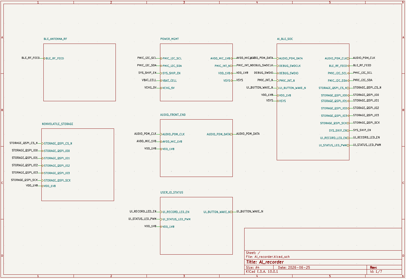
The magnetic AI microphone KiCad project includes a dedicated power-management sheet generated from the product brief. It shows the system path from the 5 V charging input through a single-cell charger and load switch to the protected VSYS rail. An ST1PS01DJR synchronous buck stage then creates the always-on VDD_1V8 rail, followed by an RC-isolated analog microphone rail.

| Project item | Verified schematic/BOM evidence | Engineering review still required |
|---|---|---|
| U3 regulator | ST1PS01DJR, with D1=0 and D0=0 documented for a 1.8 V output | Confirm the exact orderable variant, pin mapping, operating corners, availability, and assembly process |
| Input capacitor | C8, 4.7 µF on the buck input rail | Verify effective capacitance under bias, voltage rating, ripple current, and placement |
| Inductor | L1, 2.2 µH with a BOM target of at least 0.8 A saturation current | Check peak/RMS current, DCR, bias curve, tolerance, temperature, core loss, and fault behavior |
| Output capacitors | C9, 10 µF bulk plus C10, 0.1 µF high-frequency bypass on VDD_1V8 | Confirm the effective output-capacitance range, stability, ripple, and load-transient performance |
| Analog branch | R4, 1 Ω with C11, 4.7 µF and C12, 0.1 µF to form AVDD_MIC_1V8 | Validate microphone-current transients, rail noise, filter loss, and separation from switching currents |
The ST1PS01 data sheet identifies a 1.8 V to 5.5 V input range, up to 400 mA output capability, selectable outputs, power-good, and a typical 2.2 µH external inductor. Those facts make the selected device plausible for this low-power rail, but they do not prove that the generated project meets every system requirement. The schematic and BOM remain a first engineering draft; the exact variant, operating states, layout, thermal performance, noise, sourcing, and hardware results must be reviewed before production.
Common Buck Converter Circuit Mistakes
- Choosing the regulator from nominal input and load values instead of the full operating and fault range.
- Assuming the advertised output current is continuously available without checking input voltage, duty cycle, package temperature, copper area, and current limit.
- Copying an inductor value without checking saturation, RMS current, DCR, bias, tolerance, and temperature.
- Using the printed ceramic-capacitor value instead of its effective capacitance at the applied DC voltage.
- Adding output capacitance beyond the regulator’s compensated range because “more capacitance is safer.”
- Leaving enable, mode, voltage-select, or power-good pins without a documented default state.
- Routing feedback beside the switch node or sensing output before the intended load connection.
- Drawing local input capacitors but failing to reserve a genuinely compact high-di/dt loop in layout.
- Ignoring reverse current, hot plug, prebiased output, startup sequencing, or what happens when another rail powers the load first.
- Treating a correct DC output reading as proof of ripple, transient, thermal, stability, and EMI performance.
How SpeedUp Fits
SpeedUp can turn a product brief into an electronics architecture and structured, editable KiCad schematic sheets. For a buck-powered device, the brief should state the source, complete input range, output rails, current by operating state, load transients, enable and sequencing behavior, sensitive loads, protection environment, space constraints, and any preferred regulator family. The generated first draft can then expose the power path, candidate components, net names, control assumptions, BOM context, and review notes in one editable project.
SpeedUp does not replace regulator selection calculations, loop-stability work, PCB power layout, simulation, thermal analysis, EMI work, sourcing approval, safety/compliance review, manufacturing, or bench validation. Engineers remain responsible for checking the design against vendor documentation and the real product requirements.
Related SpeedUp Guides and Projects
- Schematic Diagrams: How to Read, Create, and Organize Circuits — organize power, control, and interface decisions into reviewable sheets.
- nRF54L15 KiCad Schematic Project — another real SpeedUp-generated project with a dedicated power-input sheet and editable engineering files.
FAQ
What is a buck converter circuit?
It is a non-isolated switching DC-DC circuit that regulates an output voltage below its input voltage. The power stage uses switching devices, an inductor, and capacitors; a controller adjusts duty cycle from feedback or a configured output setting.
What is the difference between a buck converter and an LDO?
An LDO regulates by dissipating the input-to-output voltage difference as heat, while a buck converter transfers energy through switching and an inductor. A buck converter is often more efficient when the voltage drop or load current is substantial, but it adds switching ripple, EMI, components, and layout complexity. The best choice depends on efficiency, noise, dropout, cost, area, and load behavior.
How do I choose the inductor for a buck converter?
Start with the regulator data sheet’s allowed or recommended inductance, estimate ripple across the real input and switching-frequency range, and calculate peak current. Then choose a part whose saturation and RMS ratings, DCR, core loss, bias behavior, tolerance, temperature range, size, and availability meet the application with margin.
Why does buck converter PCB layout matter so much?
The converter contains fast voltage edges and pulsed current loops. Parasitic inductance and capacitance can create ringing, overshoot, ground bounce, noise coupling, and EMI. The input capacitor, switches, inductor, output capacitor, ground returns, and feedback path must be placed and routed according to the regulator vendor’s guidance.
Can I copy the buck converter circuit from a data sheet?
Use the data-sheet application circuit as a starting point, but do not copy it without checking its test conditions. Your input source, output load, voltage setting, capacitor derating, inductor current, switching mode, startup sequence, fault environment, PCB stackup, cooling, and EMI target may be different. Preserve the vendor’s critical layout and compensation guidance, then validate the final hardware.
Start Your Buck Converter Project
Turn your power requirements into a reviewable buck-converter schematic draft.
Use SpeedUp to turn the product requirements into structured schematic sheets and an editable KiCad first draft for engineering review. Create a free account to begin.
Comments
No comments yet.
Leave a Reply