
Quick Answer
A decoupling capacitor supplies short bursts of current near an IC and gives high-frequency noise a low-impedance path away from the power pin. Start with the component datasheet or reference design; a 100 nF ceramic capacitor at each relevant supply pin is a common pattern, not a universal rule. Add the local and bulk capacitance required for the device, rail, regulator, and load-transient conditions, then place the high-frequency capacitor close to the pin with a short power-and-ground loop.
The schematic must show the correct values and rail assignments, but PCB placement determines whether those capacitors work at high frequency. A capacitor drawn beside an IC can still be ineffective if layout adds a long trace, shared via, narrow return path, or large loop area. Review the schematic, datasheet, package, and PCB together before treating the power network as complete.
What a Decoupling Capacitor Actually Does
Digital gates, radios, converters, displays, sensors, and analog circuits do not draw perfectly steady current. Their demand changes with clock edges, switching states, transmissions, conversions, and load steps. The upstream regulator and board-level power plane cannot respond to every fast event without some voltage movement because traces, planes, packages, and vias all have resistance and inductance.
A local capacitor stores charge near the load. During a fast current step, it helps hold the supply voltage while current from the wider power network catches up. It also lowers the local power-distribution-network impedance over part of the frequency range. Analog Devices’ MT-101 decoupling tutorial explains why real capacitors have equivalent series resistance, equivalent series inductance, and a self-resonant frequency; above resonance, adding nominal capacitance alone does not guarantee lower impedance.
This is why “put one capacitor somewhere on the 3.3 V rail” is not a complete design instruction. The useful question is: which current transient is being supported, at which pin, over which frequency range, through what physical loop?
Decoupling Capacitor vs. Bypass Capacitor
Engineers often use decoupling capacitor and bypass capacitor interchangeably. Both usually describe a capacitor from a supply rail to its return node, placed so high-frequency current circulates locally instead of through a larger shared path.
When a distinction is made, decoupling emphasizes isolating one circuit block from disturbances created by another, while bypass emphasizes giving AC noise a low-impedance path around the load or into the return plane. In practical schematic and PCB review, the naming difference is less important than the capacitor’s value, dielectric, voltage bias, package, location, and current loop.
Decoupling Capacitor Schematic and PCB Checklist
| Review area | What to check | Common failure |
|---|---|---|
| Datasheet requirement | Record every required capacitor value, rail, pin group, dielectric, ESR condition, and placement note. | Copying a generic 100 nF rule and missing a device-specific DEC, VCAP, AVDD, or regulator capacitor. |
| One capacitor per pin or group | Determine whether supply pins may share a capacitor or need dedicated local parts. | One remote capacitor is assigned to several fast power pins without a verified reference layout. |
| Capacitance under bias | Check effective capacitance at DC voltage, temperature, tolerance, and aging—not only the printed value. | A small high-value MLCC loses much of its capacitance at operating voltage. |
| Package and dielectric | Choose a suitable ceramic dielectric and package with acceptable ESR, ESL, voltage rating, and reliability. | Treating all 100 nF or 10 µF capacitors as electrically equivalent. |
| Placement | Put the highest-frequency local capacitor close to its power pin and return connection. | The schematic looks correct, but layout places the capacitor behind a long neck or on the opposite side with distant vias. |
| Loop geometry | Minimize the pin–capacitor–return loop with short, wide connections and nearby vias or planes. | Sharing a long ground via path or routing a narrow trace around another component. |
| Bulk capacitance | Add rail-, connector-, regulator-, or load-level energy storage where slower transients require it. | Expecting one tiny local capacitor to support a radio burst, motor step, display load, or long cable. |
| Regulator stability | Keep regulator input/output capacitors separate from generic bypass assumptions and follow the stability requirements. | Substituting value or ESR without checking the regulator datasheet and layout. |
| Verification | Review the PCB, BOM, rail ripple, startup, resets, emissions, and worst-case load transients. | Assuming ERC or a clean bench startup proves the power network is robust. |
Planning power integrity for a new board?
Describe the ICs, supply rails, switching loads, operating states, decoupling requirements, and layout constraints. Create a free account to start a reviewable, editable KiCad first draft.
How to Choose Decoupling Capacitor Values
1. Follow the exact datasheet and reference circuit first
A 100 nF ceramic capacitor is a widely used starting point for digital supply pins, but it is not a replacement for device documentation. Some ICs require a particular capacitor on an internal regulator, charge pump, reference, core rail, or analog supply. A regulator may specify an output-capacitance range and ESR condition for stability. An RF SoC may give package-specific component values and layout files. Those requirements outrank a generic checklist.
For example, Nordic Semiconductor’s nRF52832 reference circuitry tells designers to use the recommended package reference circuit and place the VDD bypass network close to the IC. The exact values and connections vary with device configuration and package, which is why copying a superficially similar Nordic circuit is unsafe.
2. Separate high-frequency local capacitance from bulk energy storage
A small ceramic capacitor near an IC pin has low mounting inductance and supports fast edges. A larger capacitor supports slower load changes and rail droop, but a physically larger package or remote location can reduce its usefulness at high frequency. Many boards therefore use a combination such as a local 100 nF part plus 1 µF, 4.7 µF, 10 µF, or more at the device, rail, regulator, or connector level.
Do not turn that example into a fixed recipe. Use transient current, allowable ripple, regulator response, plane impedance, and component models to decide the network. If several values are used, check their combined impedance and damping; “more decades of capacitance” can create anti-resonance peaks instead of a perfectly flat low-impedance rail.
3. Check the effective capacitance of the real part
MLCC capacitance can change with DC bias, temperature, tolerance, aging, and package stress. A 10 µF capacitor in a small package may provide substantially less than 10 µF at its operating voltage. Review the manufacturer’s bias curve and choose voltage rating, dielectric, case size, and nominal capacitance with enough margin for the application.
4. Treat analog, RF, switching, and sensitive reference rails separately
An ADC reference, PLL supply, RF rail, switching-converter input, op-amp supply, and ordinary GPIO rail may need different values, filtering, grounding, or isolation. Ferrite beads and series resistors are not automatically beneficial; they create another impedance element and can introduce resonance or DC drop. Use them only when the device guidance or power-integrity analysis supports the network.
Placement and PCB Layout Matter More Than Schematic Proximity
A schematic does not encode physical distance. Drawing C1 directly beside U1 does not guarantee that the board places it beside the correct pin. During placement review, trace the complete transient-current loop: device power pin, capacitor power pad, capacitor ground pad, ground return, and back into the device.
Texas Instruments’ CC13xx/CC26xx hardware and PCB guidance recommends placing decoupling capacitors close to the pin, keeping the return short and direct, and using separate ground vias to reduce noise coupling. Microchip’s decoupling-capacitor guidance similarly emphasizes close placement, low-ESR ceramic parts, short traces, and routing power through the capacitor before the device where applicable.
Practical layout checks include:
- Place the local capacitor on the same layer as the IC when package and reference-layout guidance allow it.
- Keep power and ground connections short and wide; avoid a long narrow trace between the capacitor and pin.
- Put ground and power vias close to capacitor pads when planes are used.
- Avoid sharing one long via or necked connection among several high-frequency capacitors.
- Keep the return path continuous; do not cross a plane split or force current around a gap.
- Give the smallest, highest-frequency local capacitor placement priority when several values are specified.
- Copy a validated reference layout when the vendor identifies a critical regulator, RF, or high-current loop.
These checks belong in a broader schematic-to-PCB layout review. Component values, reference designators, footprints, placement constraints, planes, vias, and measurement access all need to survive the handoff into board layout.
Example From a Real SpeedUp Project
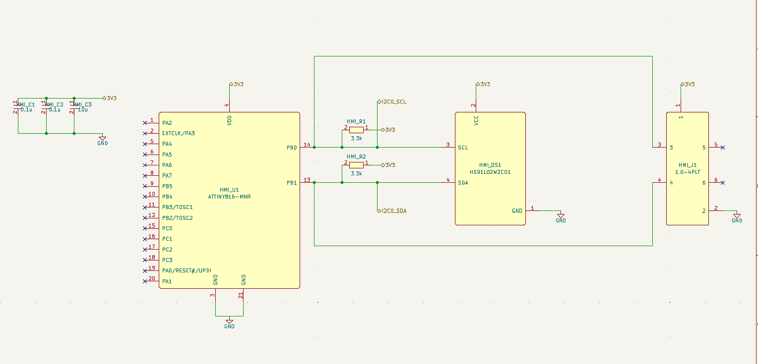
The featured schematic at the top of this guide comes from SpeedUp’s temperature and humidity sensor KiCad project. The control/display sheet places three capacitors on the controller’s 3.3 V supply: one 0.1 µF part and two 1 µF parts. It also shows the ATTINY816, I²C pull-ups, OLED supply, and ground connections in one reviewable block.
That is useful schematic evidence: the local capacitors exist, have values, and connect to the intended rail. It is not yet proof of effective high-frequency decoupling. Before production, the PCB reviewer still needs to confirm which capacitor belongs to which power pin or load, physical distance, trace and via geometry, effective capacitance under bias, regulator requirements, OLED load steps, and the return path.
A second example: why the exact device matters

The published Nordic development-board concept contains a generated target sheet with several 0.1 µF capacitors plus 1 µF and 4.7 µF parts. The visible grouping makes power-pin review easier, but the sheet uses an nRF52832 surrogate because the exact nRF54L15 symbol was not available in that generation. The lesson is not to reuse those values for nRF54L15. The lesson is to expose every rail and capacitor, then replace proxies and validate the exact device, package, reference circuitry, and layout before production.
How to Verify Decoupling on a Real Board
Visual inspection is the first check. Confirm that every schematic capacitor exists in the BOM and layout, uses the intended footprint, connects to the correct rail, and sits beside the intended power pin or pin group. Inspect the entire return path in the PCB editor rather than judging placement from component distance alone. A capacitor can look close while a plane split, distant via, narrow neck, or indirect route makes its loop electrically long.
On the bench, reproduce the operating events most likely to disturb the rail: processor wake-up, radio transmit, display refresh, sensor conversion, USB connection, motor or relay switching, and maximum simultaneous load. Watch for brownout resets, corrupted communication, ADC shifts, clock instability, unexpected emissions, or faults that disappear when a probe or extra capacitor is attached.
Measure supply ripple and transients with an appropriate probe connection. A long oscilloscope ground lead forms a large loop and can display ringing that belongs to the probe rather than the board. Use a short ground spring, coaxial tip, or dedicated measurement connector where the bandwidth and voltage allow it. Probe at the IC supply and return pins when possible, then compare the regulator output and other rail locations. Set bandwidth limits deliberately and document the measurement setup so results are repeatable.
If the design is sensitive or high speed, review the power-distribution network with impedance models, vendor capacitor data, or simulation. Include package and mounting inductance instead of treating capacitors as ideal values. Validate worst-case voltage, temperature, component tolerance, regulator control-loop behavior, and population changes. A quick fix—adding another capacitor—may hide one symptom while creating startup inrush, regulator instability, or an anti-resonance peak elsewhere.
Finally, keep the verified placement constraints with the design. Add PCB notes, courtyard or rule areas, pin-specific capacitor labels, and review comments so later routing, variant creation, or component substitution does not undo the working current loop.
Common Decoupling Capacitor Mistakes
- Using 100 nF everywhere without reading the datasheet: device-specific rails and internal regulators may need different values or connections.
- Counting schematic capacitors instead of reviewing current loops: ten remote parts can be less effective than one correctly mounted local part at the frequency that matters.
- Ignoring DC-bias derating: the nominal capacitance may not survive the real operating voltage.
- Sharing vias and narrow traces: common impedance couples noise between devices and raises the high-frequency impedance.
- Placing a via between the capacitor and power pin without analysis: the extra inductance can weaken the local path.
- Combining regulator capacitors with generic bypass parts: regulator input/output networks may have stability, ripple-current, and ESR requirements.
- Adding many values blindly: parallel capacitors can create anti-resonance peaks and do not replace PDN analysis for demanding designs.
- Treating ERC as a power-integrity test: ERC checks connectivity rules, not transient impedance, ripple, emissions, or physical placement.
How SpeedUp Fits
SpeedUp can turn a product prompt into an editable KiCad schematic draft with named rails, IC power pins, local capacitors, bulk-capacitor blocks, and review notes. That structure helps an engineer see whether a capacitor is missing, attached to the wrong rail, assigned an unexplained value, or disconnected from the intended functional block.
The generated result remains a first engineering draft. Engineers still verify the exact datasheet, reference design, symbols, footprints, capacitor part numbers, effective capacitance, regulator stability, PCB placement, return paths, signal integrity, thermal behavior, EMC, sourcing, manufacturing, and compliance. Use the complete schematic review checklist to keep those checks connected to the rest of the design.
FAQ
What is the purpose of a decoupling capacitor?
It supplies local transient current and lowers the supply impedance over part of the frequency range. This helps reduce voltage droop, noise coupling, false resets, jitter, analog error, and emissions caused by fast load-current changes.
Is 0.1 µF the standard decoupling capacitor value?
A 0.1 µF or 100 nF ceramic capacitor is common at digital IC power pins, but it is only a rule of thumb. Follow the device datasheet and reference layout, then account for package, dielectric, voltage bias, rail behavior, frequency, and the need for larger local or bulk capacitance.
Does every power pin need its own decoupling capacitor?
Many fast devices require one capacitor per power pin or per closely grouped pin set, but the correct answer is device- and package-specific. Do not merge capacitors just because the pins share a rail name; check the reference circuit and layout guidance.
How close should a decoupling capacitor be to an IC?
As close as required to minimize the high-frequency current loop, preferably following the vendor’s reference layout. There is no universal distance that fits every package and frequency. Connection geometry, vias, planes, and return-path continuity matter as much as the distance measured in millimeters.
Can one bulk capacitor replace several small bypass capacitors?
Usually not. A bulk capacitor may support slower rail transients, while small local capacitors provide lower mounting inductance near fast power pins. The final network should be based on the device requirements and power-distribution impedance, not nominal capacitance alone.
Start Your Power-Aware KiCad Project
Make decoupling and rail requirements visible in a structured schematic before PCB layout.
Use SpeedUp to turn the product requirements into structured schematic sheets and an editable KiCad first draft for engineering review. Create a free account to begin.
Comments
No comments yet.
Leave a Reply