
Quick Answer
Electronic circuit design is the process of turning required product behavior into a connected, reviewable electrical implementation. A practical workflow starts with measurable requirements, converts them into functional blocks and power domains, selects components with their supporting circuits, defines every interface, and then captures the design in structured schematic sheets. The result should explain not only which parts connect, but why each circuit exists and which assumptions still need validation.
For a modern hardware product, the useful output is more than a static circuit diagram. It includes an electrical block diagram, power and interface decisions, named nets, component and BOM context, and an editable schematic project that another engineer can open and revise. That package is still a first engineering draft. PCB layout, firmware integration, detailed calculations, component sourcing, safety, RF work, testing, compliance, and manufacturing preparation remain separate engineering responsibilities.
Why Electronic Circuit Design Matters
A circuit can be drawn neatly and still implement the wrong product. The common failure is not a missing line on the page; it is a decision that was never made. A battery-life goal may not have been translated into operating states. A sensor may have been selected before its accuracy, supply, interface, placement, and calibration needs were known. A connector may expose signals without protection or a return path. A processor may have enough pins in total but not enough compatible pins for the chosen peripherals.
Electronic circuit design creates traceability between product intent and electrical detail. Requirements decide the architecture. Architecture decides the power tree, compute platform, interfaces, and subsystem boundaries. Those decisions then become component circuits, nets, connectors, and schematic sheets. When that chain is visible, reviewers can challenge an assumption before it becomes a PCB respin, firmware workaround, enclosure change, or sourcing problem.
The process is also a handoff mechanism. Product teams can verify behavior and constraints; hardware engineers can inspect circuits and interfaces; firmware engineers can see boot, reset, interrupt, bus, and power-control assumptions; mechanical teams can find connectors, antennas, sensors, displays, and heat sources; and sourcing teams can review the proposed BOM. The schematic is valuable because it makes those decisions concrete enough to discuss.
Electronic Circuit Design Workflow
Use the workflow below as a design sequence, not a set of independent tasks. A change to battery chemistry can affect regulation, charging, protection, enclosure volume, thermal behavior, firmware states, and the BOM at the same time.
| Stage | Main decision | Reviewable output |
|---|---|---|
| 1. Requirements | What must the product do, under which constraints? | Prioritized requirements and assumptions |
| 2. Architecture | Which functional blocks and flows implement the behavior? | Circuit block diagram |
| 3. Power and states | How is the product powered, controlled, and protected? | Power tree, preliminary budget, state table |
| 4. Components | Which parts and surrounding circuits meet the requirements? | Part choices with rationale and open items |
| 5. Interfaces | How do blocks exchange power, data, control, and status? | Interface and ownership table |
| 6. Schematic capture | How should the circuits be organized and connected? | Structured schematic sheets |
| 7. Handoff review | What is verified, provisional, or still missing? | Editable project, BOM context, review plan |
Ready to turn product requirements into a circuit?
Describe the device behavior, power sources, interfaces, connectors, operating states, and constraints. Create a free account to start a reviewable, editable KiCad first draft.
1. Turn Product Behavior Into Electrical Requirements
Begin with behavior, not a favorite microcontroller. Describe what the device senses, controls, communicates, displays, stores, or powers. Add measurable constraints: input voltage, runtime, charging time, response time, sampling rate, communication range, connector type, environmental range, enclosure limits, service access, and cost or sourcing boundaries.
Separate requirements from proposed solutions. “Measure temperature from −20°C to 60°C with ±0.5°C accuracy” is a requirement. “Use sensor X over I2C” is one proposed implementation. Keeping those categories separate makes it possible to compare parts and architectures without silently changing the product promise.
Record operating states early. A portable device may have off, charging, boot, active, idle, sleep, update, and fault states. For each state, identify which blocks are powered, which events cause transitions, which signals must have safe defaults, and what the user observes. These answers influence regulators, load switches, resets, wake pins, storage, and firmware responsibilities before any detailed circuit is drawn.
2. Create a Circuit Block Diagram
Convert the requirements into functional blocks such as power input, charging, compute, sensing, wireless communication, storage, display, actuators, external connectors, debug, and user controls. Draw the important flows between them. A useful block connection identifies whether it carries power, data, control, clock, reset, interrupt, or an external interface.
Do not use the block diagram as decoration. Use it to test completeness. Every major product behavior should map to at least one block and one interface. Every block should have a power source, an owner, and a reason to exist. If the device must wake when a sensor crosses a threshold, the diagram should reveal which sensor generates the event, which rail remains available, where the interrupt goes, and which processor state handles it.
A block diagram is intentionally less detailed than a schematic. It defines the system and its boundaries; the schematic defines components, pins, nets, values, and power connectivity. The schematic diagrams guide explains those drawing types and how to read and organize the resulting circuit sheets.
3. Design the Power Tree and Operating States
List every possible energy source: battery, USB, adapter, vehicle rail, upstream connector, or harvested energy. For each source, record the normal range, abnormal conditions, polarity or backfeed risks, hot-plug behavior, peak current, charging path, and expected protection. Then define every generated rail by voltage, tolerance, current, noise sensitivity, enable behavior, and the loads it powers.
Build a preliminary power budget with active, average, sleep, and peak values. Average current alone can hide a radio transmit burst, display refresh, motor startup, or processor workload that determines the regulator and decoupling strategy. Note which loads can occur simultaneously and which firmware can schedule. Mark estimates clearly until measurements or detailed calculations replace them.
Connect the power tree to the operating-state table. Identify which rails are always on, which are switched, who controls each enable, what defaults exist before firmware starts, and how shutdown or fault recovery works. For a deeper system-level method, the embedded system architecture guide covers power, compute, interfaces, and hardware–firmware ownership before schematic implementation.
4. Select Components With Their Supporting Circuits
A component choice is not only a part number. Selecting an MCU also selects power domains, clocks, reset and boot behavior, programming access, package constraints, decoupling, and peripheral limitations. Selecting a sensor brings supply requirements, interface voltage, accuracy, calibration, placement, thermal exposure, and firmware behavior. Selecting a radio brings matching, antenna, grounding, keepout, certification, and layout work.
Use current manufacturer documentation for each critical part. Compare electrical limits, recommended circuits, reference designs, package variants, lifecycle, and availability. Record whether a surrounding value comes from a calculation, a reference design, a previous validated product, or an assumption that still needs review. That provenance matters when the design changes.
Check the complete subsystem rather than optimizing one device in isolation. A low-power sensor may not improve battery life if its regulator has high standby current. A cheaper connector may increase board area or assembly risk. A processor module may reduce RF work but add cost and mechanical constraints. Electronic circuit design is a system tradeoff, not a sequence of independent component searches.
5. Define Every Interface Before Assigning Pins
Create an interface table for every connection between blocks. Capture the protocol, direction, voltage domain, expected speed, pull-up or termination ownership, interrupt or wake behavior, connector exposure, cable assumptions, and firmware owner. Include power enables, reset lines, status signals, and test access—not only familiar buses such as I2C, SPI, UART, USB, or CAN.
Allocate the non-negotiable pins first: power, ground, clocks, reset, debug, analog inputs, RF, high-speed interfaces, and peripherals with limited routing options. Then assign flexible GPIO. Reserve programming, recovery, and factory-test paths before convenient pins and connector positions disappear.
Use signal names that express purpose and active level. Names such as DISPLAY_PWR_EN, SENSOR_INT_N, DEBUG_UART_TX, and BATTERY_LOW_N communicate more than a temporary pin number. A stable functional name also lets the pin mapping change without erasing the design intent.
6. Capture the Design in Structured Schematic Sheets
Organize the schematic by stable responsibility. A connected device might use separate sheets for power input, compute and wireless, sensing, display, storage, external interfaces, and user controls. The goal is not to maximize the page count. It is to make each subsystem understandable and to expose the signals that cross its boundary.
Make the top-level sheet an interface map. It should show the main blocks, generated rails, buses, control signals, interrupts, resets, and connector-facing paths without repeating every local component. Detailed sheets should contain the support circuits, values, notes, references, and local connectivity required to review that function.
KiCad supports hierarchical sheets, sheet pins, hierarchical labels, global labels, buses, and reusable design blocks. The current KiCad Schematic Editor documentation describes how those elements work. Use hierarchy to make interfaces visible, not to hide connectivity behind broad global scope.
Keep notes close to the decisions they qualify. Mark provisional components, unverified footprints, calculated values, reference-design values, voltage-domain assumptions, firmware dependencies, and layout-sensitive circuits. A reviewer should be able to distinguish intentional design from unresolved scaffolding without searching a separate message thread.
7. Review the BOM, Symbols, Footprints, and Handoff
The schematic and BOM should describe the same design. Check that each orderable part has the intended value, package, lifecycle status, and sourcing context. Verify that schematic symbols match the selected package and that footprints match the manufacturer drawing. Confirm polarity, pin numbering, exposed pads, mounting holes, connector orientation, and any mechanical features that affect the board or enclosure.
Separate what the schematic proves from what still requires downstream work. It can make intended connectivity, part context, interfaces, and design assumptions reviewable. It does not prove signal integrity, thermal performance, RF behavior, mechanical fit, firmware correctness, safety, compliance, manufacturability, or performance in a physical prototype.
Package the handoff so another engineer can continue: project file, schematic sheets, local libraries when required, BOM, source references, design notes, and a list of open decisions. An editable project is more useful than an exported image because reviewers can inspect hierarchy, search nets, replace parts, update footprints, and preserve revisions. The KiCad schematic generator workflow shows how a product brief can become that kind of structured starting point.
Example From a Real SpeedUp Project
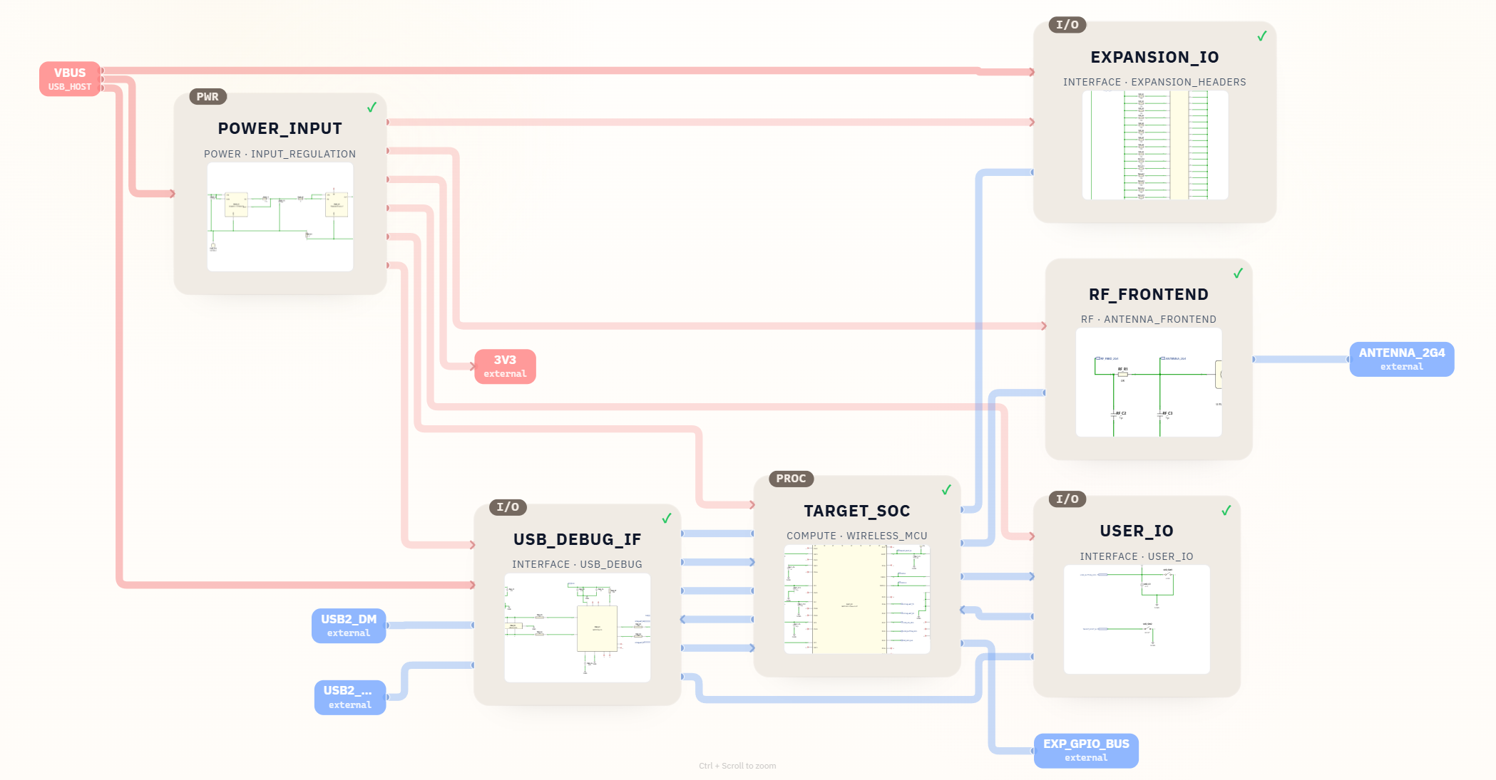
The nRF54L15 development board KiCad project shows how a short hardware request can be expanded into reviewable electronic design artifacts. The source prompt asked for an nRF54L15 development board. SpeedUp produced a circuit block diagram, a KiCad project named nrf54db, a top-level schematic, six named module sheets, BOM files, local symbol and footprint libraries, and a downloadable review package.

The sheet hierarchy makes the design easier to inspect. POWER_INPUT handles USB power, protection, regulation, and test access. USB_DEBUG_IF covers the USB-C debug path and USB-to-UART bridge. TARGET_SOC contains the processor area, clocks, decoupling, debug, and signal breakout. RF_FRONTEND contains the 2.4 GHz path, while EXPANSION_IO and USER_IO expose development and interaction functions.
The example is useful because it also exposes a critical unresolved decision. The generated BOM uses an nRF52832 QFN-48 device as a provisional surrogate for the requested nRF54L15. That symbol, package, pin mapping, power arrangement, clocks, and RF implementation must be replaced or validated against Nordic’s current package-specific documentation. Nordic publishes separate nRF54L15 pin assignments for the supported packages; there is no package-independent mapping that can be copied blindly.
That is the correct role for a first engineering draft. It creates an editable structure, names the subsystems, connects the intended interfaces, provides BOM context, and gives reviewers concrete files to challenge. It is not the official Nordic development kit, a validated RF design, a routed PCB, or a production-ready reference. The visible substitution becomes an explicit review task rather than an invisible assumption.
Electronic Circuit Design Handoff Checklist
| Review area | Minimum evidence before handoff |
|---|---|
| Requirements | Prioritized behavior, measurable limits, assumptions, and unresolved choices |
| Architecture | Functional blocks with named power, data, control, and external interfaces |
| Power | Sources, rails, preliminary current budget, enables, sequencing, and protection assumptions |
| Components | Part rationale, surrounding circuits, current documentation, and substitution notes |
| Interfaces | Protocol, direction, voltage, speed, ownership, connectors, and safe defaults |
| Schematic | Readable hierarchy, named nets, values, references, notes, and explicit boundaries |
| Libraries | Verified symbols, footprints, packages, polarity, pin numbering, and mechanical features |
| BOM | Orderable parts, quantities, alternates, lifecycle, availability, and provisional entries |
| Open work | Owners for calculations, layout, firmware, test, sourcing, safety, compliance, and manufacturing |
Common Electronic Circuit Design Mistakes
- Starting with a preferred part. This forces the product around an MCU, sensor, regulator, or radio before behavior, interfaces, power, and lifecycle constraints are known.
- Using vague requirements. Words such as “low power,” “fast,” or “small” do not support circuit decisions until they become measurable ranges, states, limits, and priorities.
- Drawing blocks without interfaces. A box-and-arrow picture is not an electrical architecture when it omits voltage, direction, protocol, ownership, control behavior, and return paths.
- Selecting the main IC but ignoring its ecosystem. Clocks, reset, boot, decoupling, programming, protection, connectors, and reference-design constraints belong to the component decision.
- Leaving firmware assumptions implicit. Enables, resets, wake signals, interrupts, updates, recovery, and fault behavior need safe defaults before firmware runs.
- Treating symbols and footprints as clerical details. Package and pin mismatches can invalidate an otherwise plausible circuit before layout begins.
- Copying a reference circuit as the entire product. Manufacturer guidance may solve one component’s implementation, but it does not define the complete power, interface, mechanical, firmware, sourcing, and validation plan.
- Calling the first schematic finished. A reviewable first draft improves the starting point; it does not replace physical implementation and validation.
How SpeedUp Fits
SpeedUp helps turn a plain-language hardware brief into an electronics system architecture and a structured schematic draft. The workflow can expose functional blocks, power paths, interfaces, named schematic sheets, component context, BOM information, and an editable KiCad project instead of stopping at a static drawing.
That makes early electronic circuit design more concrete. Engineers can review an actual rail, component, net, connector, sheet, or BOM line. Product and firmware teams can see which requirements and control assumptions are represented. Missing information becomes a named review item that can be corrected in the source project.
Treat the generated output as a first engineering draft for review. Qualified engineers still verify the architecture, calculations, component choices, manufacturer guidance, symbols, footprints, power behavior, analog and RF details, PCB layout, firmware, sourcing, safety, testing, compliance, and manufacturing outputs before release.
Related Project Examples
- ESP32 E-Ink MQTT display schematic — a connected display example with power input, Wi-Fi compute, and a protected display interface.
- The nRF54L15 development-board example above provides a deeper look at a six-sheet KiCad hierarchy, BOM context, and explicit component-substitution review.
FAQ
What is electronic circuit design?
Electronic circuit design is the process of converting required behavior and constraints into an electrical architecture, component circuits, interfaces, and schematic documentation. It includes requirements, power, component selection, connectivity, and handoff decisions—not only drawing symbols.
What are the main steps in the electronic circuit design process?
Define measurable requirements, create a functional block diagram, design the power tree and operating states, choose components with their support circuits, define interfaces and ownership, capture the schematic in structured sheets, and review symbols, footprints, BOM data, and unresolved work before PCB layout.
What software is used for electronic circuit design?
Engineers use schematic and PCB design tools such as KiCad and commercial EDA platforms, along with calculation, simulation, documentation, version-control, and sourcing tools. The right tool depends on the design, but the engineering decisions should remain visible and editable rather than locked inside a static image.
What is the difference between circuit design and a circuit diagram?
Circuit design is the decision process that selects architecture, parts, values, interfaces, and constraints. A circuit diagram or schematic is one artifact produced by that process. A drawing can show connectivity, but the design also includes requirements, calculations, source evidence, BOM context, physical constraints, and validation plans.
Can AI design an electronic circuit?
AI-assisted tools can transform a detailed hardware brief into an initial architecture, component context, and editable schematic draft. The result can accelerate review and iteration, but engineers must still validate the electrical design, documentation, symbols, footprints, layout constraints, firmware assumptions, sourcing, safety, testing, compliance, and manufacturing readiness.
What comes after schematic design?
After the schematic is reviewed, teams complete PCB stack-up and layout, mechanical integration, firmware, sourcing, prototype assembly, bring-up, measurement, functional and environmental testing, safety and compliance work, design revisions, and manufacturing documentation. The exact sequence depends on product risk and regulatory requirements.
Start Your Electronic Circuit Design
Move from product requirements to a structured, editable KiCad starting point.
Use SpeedUp to turn the product requirements into structured schematic sheets and an editable KiCad first draft for engineering review. Create a free account to begin.
Comments
No comments yet.
Leave a Reply