
Quick Answer
An embedded system architecture is the working map that connects product requirements to hardware blocks, firmware responsibilities, interfaces, power states, and engineering files. For a hardware product, it should show how power enters and moves through the device, which processor controls each function, how sensors, displays, radios, storage, and connectors communicate, and where the design still contains assumptions.
Build the architecture before detailed schematic capture. Start with required behavior and operating states, create the power tree, select the compute platform, map interfaces, assign hardware-versus-firmware ownership, and then translate the blocks into organized KiCad sheets with named connections. The output is not a production release. It is a reviewable plan that lets product, hardware, firmware, mechanical, sourcing, and test teams find missing decisions before they become expensive board changes.
Why Embedded System Architecture Matters
A schematic can be electrically detailed and still describe the wrong product. The failure usually begins earlier: a battery life target was never translated into operating states, a display voltage was assumed rather than specified, two peripherals were assigned to incompatible pins, a connector omitted a return path, or a firmware-controlled rail had no defined startup behavior. Once those decisions are buried across several schematic sheets, changing them can affect component selection, board area, routing, firmware, enclosure openings, and the BOM at the same time.
Architecture provides the layer between a product idea and individual circuits. It turns statements such as “portable,” “connects to a phone,” or “runs for a week” into questions that engineering can answer: What is the energy source? Which radio and protocol are required? What wakes the system? Which rails remain powered during sleep? Where is data stored? Which external connectors are user accessible? What must happen when the battery is low or communication fails?
The goal is not to create a decorative embedded system block diagram. The goal is to make every important product behavior traceable to a hardware block, interface, operating state, or clearly labeled unresolved item.
Embedded System Architecture Framework
A useful architecture review covers nine connected areas. The table below can be used as a first-pass checklist before schematic capture begins.
| Architecture area | Questions to answer | Expected artifact |
|---|---|---|
| Product behavior | What must the device sense, control, display, store, or communicate? | Prioritized functional requirements |
| Operating states | What happens during off, charging, boot, active, idle, sleep, update, and fault states? | State and transition table |
| Power architecture | What are the sources, rails, peak loads, sequencing, protection, and shutdown paths? | Power tree and preliminary budget |
| Compute platform | Which MCU, processor, module, memory, clocks, and debug path are required? | Compute block with selection rationale |
| Functional blocks | Which sensing, actuation, display, audio, storage, or radio functions need dedicated circuits? | Subsystem list and boundaries |
| Interfaces | Which buses, voltage domains, speeds, connectors, and signal directions connect the blocks? | Interface and pin-allocation table |
| Hardware-firmware boundary | Who controls power, timing, calibration, recovery, security, and user-visible behavior? | Ownership and startup assumptions |
| Physical constraints | What limits board size, connector placement, heat, antenna clearance, airflow, or ingress protection? | Mechanical and layout constraint notes |
| Engineering handoff | Which decisions, files, and open risks must move into schematic, firmware, layout, sourcing, and test work? | Traceable architecture package |
Defining an embedded hardware product?
Describe the product behavior, operating states, power architecture, compute, interfaces, sensors, connectivity, and constraints. Create a free account to start a reviewable, editable KiCad first draft.
1. Start With a Hardware Product Brief
A useful brief describes product behavior without prematurely locking every component. State who uses the device, what it must do, where it operates, how it is powered, which external systems it connects to, and which constraints cannot move. Include measurable targets when they exist: input voltage range, battery type, expected runtime, sensor sample rate, communication distance, startup time, storage duration, enclosure size, connector type, or environmental range.
Separate requirements from preferences. “Must operate for seven days between charges” is a requirement. “Use a 500 mAh cell” is a proposed solution and may conflict with the runtime, enclosure, or radio duty cycle. “Needs wireless connectivity” is incomplete; the architecture changes depending on whether the product needs BLE provisioning, continuous Wi-Fi, long-range sub-GHz communication, cellular coverage, or only a service-mode connection.
A compact brief should also list unknowns. Unknowns are not failures if they are visible and assigned. They become expensive when the schematic silently selects a value, connector, or protocol that the product team never approved.
2. Define Operating States Before Choosing Parts
Operating states connect user behavior to power and firmware. A battery device may have shipping, off, charging, boot, active measurement, radio transmit, idle, deep sleep, firmware update, and fault states. A mains-powered controller may instead need normal operation, standby, brownout recovery, maintenance, and safe shutdown.
For each state, record which blocks are powered, which clock or wake source is active, what the processor is doing, and what event causes the next transition. This exposes architecture questions early. Can the charger operate while the main processor is off? Does a sensor interrupt wake the MCU directly? Must the display retain state during sleep? Can the radio and backlight peak at the same time? What happens if external power disappears during an update?
The answers affect regulators, load switches, reset circuits, interrupt routing, nonvolatile storage, connector behavior, and firmware sequencing. They should be decided together rather than scattered across separate discipline documents.
3. Build the Power Architecture
Start the power tree at every possible source: battery, USB, adapter, vehicle supply, energy harvester, or an upstream system connector. Record the normal and abnormal input range, reverse connection risk, inrush, hot-plug behavior, charging path, and whether power can arrive from more than one source.
Then define each rail by voltage, current, noise sensitivity, startup order, always-on requirement, and control owner. A single “3V3” box is often too vague. The MCU, radio, analog sensor, display, and external connector may have different peak loads, noise constraints, or shutdown behavior even when they nominally share a voltage.
Create an initial budget using active, average, and sleep values instead of one current number. Mark loads that occur simultaneously and those that firmware can schedule. This budget does not replace detailed component calculations or measurement, but it tells the architecture whether the proposed source, regulator topology, battery, and thermal envelope are plausible enough to continue.
4. Choose Compute and Map Every Interface
Choose the MCU, processor, or module only after the device behavior and interfaces are visible. Check processing and memory needs, hardware peripherals, voltage domains, low-power modes, security requirements, debug access, lifecycle, package, module certifications where relevant, and the firmware ecosystem. A familiar MCU is not automatically the right architecture if it lacks the required high-speed interface, wake source, memory, radio, or pin capacity.
Build an interface table before assigning pins. For each connection, capture protocol, direction, voltage, maximum speed, pullup or termination needs, connector exposure, expected cable length, interrupt or wake behavior, and ownership. Treat “I2C sensor” as the beginning of a decision, not the complete decision. The bus still needs addresses, voltage compatibility, pullup ownership, speed, capacitance assumptions, and a recovery plan if a device holds a line low.
Reserve programming, debug, factory-test, and recovery access at this stage. If those paths are added after every convenient pin and connector position is consumed, bring-up becomes a mechanical and electrical redesign rather than a documentation update.
5. Compare Architecture Alternatives Before You Commit
Do not hide an important architecture choice inside a single block. When two approaches are credible, compare them explicitly before schematic capture. A wireless product might compare a certified module with a bare SoC, a battery device might compare a buck-boost rail with separate buck and boost paths, and a sensor product might compare continuous sampling with interrupt-driven duty cycling.
Use the same criteria for every option: product behavior, power, board area, component count, firmware effort, RF or analog risk, sourcing, cost, test access, schedule, and the amount of downstream validation required. Record what evidence would change the decision. This prevents a provisional choice from becoming permanent only because it was drawn first.
The comparison does not need to be a long design study. A one-page decision table with assumptions and owners is often enough. The important outcome is that the selected architecture has a documented reason and the rejected option can be revisited if a requirement, component, or schedule constraint changes.
6. Define Hardware-Firmware Responsibilities
Every controllable rail, reset line, interrupt, enable pin, multiplexer, watchdog, and status signal creates a contract between hardware and firmware. Record who owns the signal, its safe default, its behavior before firmware runs, and what should happen during a crash, brownout, update, or sleep transition.
For example, a display rail controlled by an MCU GPIO raises several questions. Does the rail remain off during reset? Is the GPIO guaranteed to have a safe state before initialization? Must the display reset line be asserted before power changes? Can the display back-power the processor through signal pins? Does firmware wait for a power-good signal or only a fixed delay? Architecture should expose these dependencies before the schematic chooses pull resistors and load-switch logic.
Keep an ownership table beside the block diagram. It should include startup order, shutdown order, fault response, calibration storage, update behavior, wake sources, and user-visible recovery. This table becomes useful to hardware and firmware teams immediately, even before the final component set is locked.
7. Turn Architecture Blocks Into KiCad Sheets
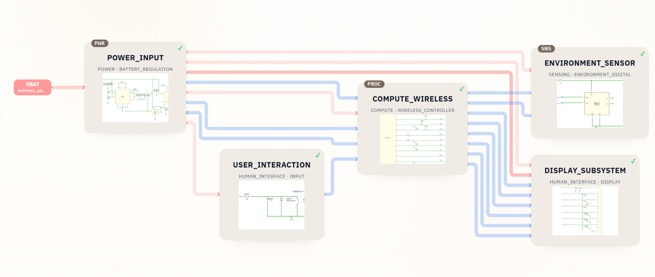
The block diagram should map cleanly into schematic organization. A practical project might use separate sheets for power input, compute and wireless, sensors, display, storage, external interfaces, and user interaction. The exact boundaries depend on the product, but each sheet should have a clear function and a small, documented interface to the rest of the design.
Name connections by purpose rather than by a temporary pin number. Signals such as DISPLAY_PWR_EN, BATTERY_LOW_N, SENSOR_I2C_SCL, and USER_EVENT_N describe ownership and behavior. The final pin mapping can then change without erasing the intent. Power rails should also be named consistently across the architecture, schematic, budget, and firmware documentation.
KiCad supports multi-sheet and hierarchical schematic organization, labels, sheet pins, and reusable sheets. Its current Schematic Editor documentation explains how sheets and connections are represented. The important architecture decision is to make subsystem boundaries visible and reviewable rather than placing the entire product on one dense page. For a wider prompt-to-files workflow, see the KiCad schematic generator guide.
Example From a Real SpeedUp Project
The Desktop Robot ESP32 KiCad project shows the difference between a product idea and a reviewable embedded system architecture. The generated project divides the controller electronics into five modules: POWER_INPUT, COMPUTE_WIRELESS, DISPLAY_SUBSYSTEM, ENVIRONMENT_SENSOR, and USER_INTERACTION.

The top-level sheet makes the scope legible. It shows controller, power, display, environmental sensing, and user input functions, but it does not pretend to be a complete robot drivetrain. The source package contains a KiCad project, five module sheets, local symbol and footprint libraries, and a BOM with 39 line items and 75 placed quantities. Those files make architecture decisions concrete enough for engineering review.
The example also exposes open work. The power design still needs regulator, transient, sequencing, thermal, and grounding validation. The ESP32 area needs boot, debug, RF keepout, interface, and firmware review. The display, sensor, and user-input blocks still depend on connector details, enclosure decisions, airflow, and firmware behavior. That is the correct boundary for an architecture-backed first schematic: specific enough to inspect and revise, but not represented as a routed, tested, compliant, or manufacturing-ready product.
Architecture-to-Schematic Handoff Checklist
| Before schematic capture | Minimum handoff evidence |
|---|---|
| Requirements | Prioritized behavior, measurable constraints, assumptions, and unresolved decisions |
| States | Power state table, wake sources, transitions, update behavior, and fault response |
| Power | Sources, rails, preliminary current budget, control signals, protection, and sequencing |
| Compute | MCU or module rationale, memory, clocks, debug, programming, and lifecycle notes |
| Interfaces | Bus, direction, voltage, speed, address, connector, pullup, termination, and wake assumptions |
| Physical constraints | Board outline inputs, antenna zones, heat sources, sensor exposure, connectors, and keepouts |
| Ownership | Hardware, firmware, mechanical, sourcing, validation, and compliance owners |
| Traceability | Every major requirement maps to a block, interface, state, or named open item |
Common Embedded System Architecture Mistakes
- Starting with the MCU. This makes the product fit the chosen processor instead of choosing compute resources from behavior, interfaces, power states, and lifecycle needs.
- Drawing boxes without interfaces. A block diagram that omits signal direction, voltage, protocol, ownership, and power does not provide enough information for schematic capture.
- Using one current number. Average current alone can hide radio, display, motor, or processor peaks that determine regulator, battery, and decoupling choices.
- Leaving firmware behavior implicit. Power enables, resets, interrupts, boot modes, updates, and fault recovery need safe defaults before firmware starts.
- Ignoring mechanical and RF constraints. Antennas, displays, microphones, sensors, connectors, heat sources, and user-accessible parts can decide the physical architecture.
- Treating a reference circuit as the complete product. Vendor guidance, such as the official ESP32 hardware design guidelines, is essential for the selected component, but it does not define the product’s complete power, interface, enclosure, firmware, sourcing, or validation plan.
- Calling the first schematic finished. Architecture and schematic generation create a better starting point; they do not replace layout, firmware integration, sourcing checks, safety work, testing, RF validation, compliance, or manufacturing preparation.
How SpeedUp Fits
SpeedUp helps move from a plain-language product brief to an electronics system architecture and structured schematic draft. The workflow can expose blocks, named interfaces, schematic sheets, component context, BOM information, and an editable KiCad project instead of stopping at a static diagram. The broader AI circuit schematic generator guide explains this prompt-to-project path.
That makes early review more concrete. A hardware engineer can point to a rail, sheet, net, connector, component, or BOM line instead of reviewing only prose. Firmware can identify control signals and startup assumptions. Product and mechanical teams can see which capabilities and physical constraints are present or missing.
Treat the generated result as a first engineering draft. Engineers still validate electrical design, component choices, symbols, footprints, power behavior, RF implementation, PCB layout, firmware, sourcing, safety, test strategy, compliance, and manufacturing outputs before release.
Related Project Examples
- nRF54L15 development board KiCad project — power input, USB debug, target SoC, RF frontend, expansion, and user I/O architecture.
- Temperature and humidity sensor KiCad project — battery power, USB-C charging, sensing, display, and low-power product decisions.
FAQ
What is embedded system architecture?
Embedded system architecture is the structured definition of a device’s hardware blocks, software responsibilities, interfaces, power states, data flow, physical constraints, and engineering boundaries. It connects product requirements to implementation decisions.
What should an embedded system block diagram include?
Include every power source and rail, compute device, memory, sensor, actuator, display, radio, storage block, connector, programming path, and user interface. Label the important protocols, voltage domains, signal directions, control ownership, and unresolved decisions.
How is architecture different from a schematic?
Architecture defines what blocks exist, why they exist, how they interact, and which requirements they satisfy. A schematic implements those decisions with specific circuits, components, nets, values, symbols, and footprints. One architecture block may become one or several schematic sheets.
Should hardware or firmware architecture come first?
Develop them together from product behavior and operating states. Hardware decisions create firmware responsibilities, while firmware timing, storage, update, recovery, and low-power needs affect component and circuit choices.
Can an architecture be generated from a product prompt?
Yes, a detailed product prompt can be transformed into an initial block architecture, interface plan, schematic hierarchy, component context, and editable project. The quality improves when the prompt includes power, behavior, interfaces, operating states, environmental constraints, preferred components, and required outputs. Engineers must still review and validate the result.
Start Your Embedded System Project
Turn your embedded product brief into a reviewable electronics architecture and KiCad draft.
Use SpeedUp to turn the product requirements into structured schematic sheets and an editable KiCad first draft for engineering review. Create a free account to begin.
Comments
No comments yet.
Leave a Reply