
Quick Answer
An ESP32 pinout is useful only after you identify the exact hardware in front of you: the ESP32 chip, an ESP32-WROOM module, or a development board built around that module. Those three layers do not share the same physical pin numbers. For a custom schematic using an ESP32-WROOM-32E, start with the module datasheet, reserve 3V3, EN, and every ground connection, then classify the remaining GPIOs by boot behavior, input/output capability, analog limitations, and peripheral routing.
The most important constraints are easy to miss in a colorful development-board diagram. GPIO34, GPIO35, GPIO36, and GPIO39 are input-only and have no internal pull resistors. GPIO0, GPIO2, GPIO5, GPIO12, and GPIO15 are sampled as strapping pins during reset. ADC2 channels conflict with Wi-Fi use on the classic ESP32, while the GPIO matrix makes many digital peripheral signals flexible rather than permanently tied to one pin. A reliable schematic therefore needs a pin-budget table, not just a pinout image.
This guide focuses on the classic ESP32-WROOM-32E module used in a real SpeedUp desktop-robot project. Newer ESP32-C, ESP32-S, ESP32-H, and ESP32-P devices have different pinouts and restrictions, so always reopen the datasheet when the exact part number changes.
Why the ESP32 Pinout Matters in a Schematic
A development board can hide several hardware decisions. Its USB-to-UART bridge may already occupy GPIO1 and GPIO3. Its BOOT and RESET buttons may control GPIO0 and EN. A regulator may allow a board-level 5 V input even though the ESP32 module itself still runs from 3.3 V. Header labels may also omit the module’s exposed ground pad and internal flash connections.
When the ESP32 moves into a custom PCB, those hidden decisions become your responsibility. The schematic has to define:
- which exact ESP32 chip or module is being used;
- how the 3.3 V rail handles radio current transients;
- how EN is biased and reset;
- what every strapping pin sees during power-up;
- which pins are inputs, outputs, analog inputs, or peripheral signals;
- how firmware will map I2C, SPI, UART, PWM, and interrupts;
- which programming and debug connections remain accessible; and
- where the module antenna and its keepout sit on the PCB.
That is why the best ESP32 pinout is not a single diagram copied into a design review. It is a documented agreement between the datasheet, the schematic, the PCB constraints, and the firmware pin map.
First Identify the Pinout Layer
| Layer | What the numbers mean | Best source | Common mistake |
|---|---|---|---|
| ESP32 chip | Package pads on the silicon device | Exact ESP32-series chip datasheet | Assuming a module exposes every chip pad |
| ESP32-WROOM module | Castellated module pins plus the exposed ground pad | Exact module datasheet and hardware design guide | Using development-board header numbers as module pins |
| ESP32 development board | Board-header positions, often labeled by GPIO name | Board revision documentation and schematic | Assuming all 30-pin or 38-pin boards are wired alike |
The ESP32-WROOM-32E module has 38 edge pins plus an exposed ground pad numbered 39. A DevKit may present 30 or 38 header positions, but those are board connector positions rather than a new version of the module pinout. Confirm the board manufacturer and revision before using any third-party diagram.
ESP32-WROOM-32E Pinout at a Glance
The table below groups the module pins by the decisions they create in a schematic. It is a planning aid, not a replacement for Espressif’s current ESP32-WROOM-32E datasheet.
| Module pin | Name / GPIO | Schematic planning note |
|---|---|---|
| 1, 15, 38, 39 | GND | Connect all ground pins and the exposed pad to the ground system with a low-impedance return. |
| 2 | 3V3 | Feed from a stable 3.3 V rail with local decoupling. Do not apply 5 V to the module supply or GPIO. |
| 3 | EN / CHIP_PU | Must not float. Define power-up and manual or automatic reset behavior. |
| 4, 5, 6, 7 | GPIO36, GPIO39, GPIO34, GPIO35 | Input-only analog-capable pins. They have no internal pull-up or pull-down. |
| 8, 9 | GPIO32, GPIO33 | General I/O with ADC1, touch, and RTC functions; useful when analog sensing must coexist with Wi-Fi. |
| 10, 11, 12 | GPIO25, GPIO26, GPIO27 | General I/O with ADC2; GPIO25 and GPIO26 also provide DAC functions on the classic ESP32. |
| 13, 14, 16 | GPIO14, GPIO12, GPIO13 | General I/O, but GPIO12 is a strapping pin and its reset state requires special care. |
| 17-22, 32 | NC on ESP32-WROOM-32E | Leave these module pins unconnected as directed by the datasheet. |
| 23, 24, 25 | GPIO15, GPIO2, GPIO0 | All are strapping pins. GPIO0 also selects normal boot versus download mode. |
| 26, 27, 28 | GPIO4, GPIO16, GPIO17 | General I/O on WROOM modules; verify availability on modules that integrate PSRAM. |
| 29, 30, 31 | GPIO5, GPIO18, GPIO19 | Often used for SPI; GPIO5 is also a strapping pin. |
| 33, 36, 37 | GPIO21, GPIO22, GPIO23 | Common choices for I2C SDA, I2C SCL, and SPI MOSI, but digital routing can be reassigned. |
| 34, 35 | GPIO3 / RXD0, GPIO1 / TXD0 | Default programming and console UART. Preserve access unless another programming strategy is defined. |
Mapping an ESP32 product?
Describe the ESP32 variant, power, boot, programming, RF, ADC, I2C, SPI, and GPIO requirements. Create a free account to start a reviewable, editable KiCad first draft.
Plan the ESP32 Pinout by Constraint, Not by Convenience
1. Reserve power, ground, EN, and programming first
Start the pin budget with the connections that are not optional. Assign every ground, the 3.3 V supply, and EN before counting available GPIOs. Add the programming path early as well. On a classic ESP32 design, GPIO1 and GPIO3 commonly carry the UART0 transmit and receive signals, while GPIO0 and EN participate in entering the serial bootloader and resetting the device.
A board can use pogo pads, a header, or an onboard USB-to-UART bridge, but the schematic should make the intended sequence clear. If another circuit drives GPIO1, GPIO3, GPIO0, or EN, check for contention during programming and reset.
2. Treat strapping pins as conditional GPIOs
GPIO0, GPIO2, GPIO5, GPIO12, and GPIO15 are sampled during reset on the classic ESP32. They can operate as normal GPIOs afterward, but external pull resistors, peripheral outputs, level shifters, and large capacitors can change the sampled level. Espressif’s ESP32 schematic checklist recommends a pull-up on GPIO0 and warns against a large capacitor there because it can force an unintended download-mode entry.
GPIO12 deserves extra attention because its reset state participates in selecting the flash supply voltage. Do not let a connected peripheral drive that node without checking the module datasheet and the complete reset timing. “It works after firmware starts” is not evidence that the power-up state is safe.
3. Keep input-only pins out of output roles
GPIO34, GPIO35, GPIO36, and GPIO39 can sense digital or analog signals but cannot drive outputs. They also lack internal pull resistors. This makes them useful for status inputs and ADC1 measurements, provided the external circuit defines a valid state. It also makes them wrong choices for LEDs, chip-select outputs, clocks, or display control lines.
In a schematic review, write the direction beside every net. A name such as POWER_GOOD communicates an input; a generic name such as STATUS does not.
4. Separate ADC1 and ADC2 decisions
The classic ESP32 exposes analog inputs across ADC1 and ADC2. If the product uses Wi-Fi, favor ADC1 pins GPIO32 through GPIO39 for measurements that must remain available while the radio is running. Espressif documents that ADC2 is shared with the Wi-Fi driver, so ADC2 readings can fail or become unavailable while Wi-Fi is active.
Analog pin selection is only the first step. The schematic still needs the expected source impedance, input range, filtering, protection, accuracy target, and calibration plan. An “ADC-capable” label does not guarantee a clean sensor measurement beside a radio and switching regulator.
5. Use the GPIO matrix deliberately
The ESP32 GPIO matrix allows many digital peripheral signals to move between available GPIOs. On a generic classic ESP32 configuration, GPIO21 and GPIO22 are common defaults for I2C SDA and SCL. A common SPI assignment is GPIO23 for MOSI, GPIO19 for MISO, GPIO18 for SCK, and GPIO5 for chip select. These are conventions, not permission to ignore the rest of the circuit.
Choose the final mapping by considering boot states, connector routing, signal direction, board congestion, interrupts, low-power behavior, and firmware support. Then keep the same names in the schematic and firmware configuration. For I2C, also size the pull-ups for bus capacitance and speed; the separate I2C pull-up resistor guide shows the calculation and review process.
6. Reserve the RF edge before the PCB exists
The WROOM-32E includes a PCB antenna and a specified keepout zone. The schematic cannot enforce placement, but it should carry a visible design note that keeps copper, components, enclosure metal, batteries, displays, and noisy switching paths away from the antenna region. Module choice and antenna orientation belong in the early architecture, not at the end of routing.
Build an ESP32 Pin-Budget Table Before Drawing Nets
A pin-budget table converts product requirements into reviewable assignments. Create it before wiring the symbol, then update it whenever the interface list changes.
| Signal | Direction | Preferred GPIO | Reset requirement | Firmware / layout note |
|---|---|---|---|---|
| I2C SDA / SCL | Bidirectional / output clock | GPIO21 / GPIO22 | External pull-ups define idle high | Confirm bus voltage, pull-up value, and connector capacitance |
| SPI display | Mostly outputs | GPIO23 / GPIO18 / reviewed CS pin | Display must not disturb a strapping pin | Add MISO only when the display or peripheral returns data |
| Analog battery monitor | Input | ADC1-capable GPIO | Known voltage during reset | Check divider current, range, filtering, and calibration |
| Power-good interrupt | Input | GPIO34-39 can be suitable | External pull may be required | Check logic polarity and wake capability |
| Programming UART | Input / output | GPIO3 / GPIO1 | No contention during reset | Expose test pads or a connector |
Add columns for connector pin, net name, peripheral instance, pull state, voltage domain, deep-sleep behavior, and verification owner when the project becomes more complex. The point is to expose conflicts before they become copper.
A practical pinout review sequence
Review the completed table in a fixed order. First, compare the symbol value and footprint against the exact ordering code in the BOM. Second, account for every power, ground, EN, NC, and exposed-pad connection. Third, highlight the five classic ESP32 strapping GPIOs and write the reset level created by the complete external circuit beside each one. Fourth, mark GPIO34 through GPIO39 as input-only and record every external pull resistor.
Next, compare analog requirements with the ADC1 and ADC2 allocation, especially when Wi-Fi will run at the same time as sampling. Trace programming and console access from GPIO1, GPIO3, GPIO0, and EN to a connector, test pads, or an automatic programming circuit. Then compare each I2C, SPI, UART, PWM, and interrupt net with the firmware pin configuration. Finally, inspect the planned physical direction of high-speed and RF-sensitive connections: a legal GPIO assignment can still create a poor layout when it forces a display clock under the antenna or places the module too close to metal.
Record unresolved items as explicit engineering questions. Examples include “Can the display drive CS during reset?”, “Must battery monitoring work while Wi-Fi transmits?”, and “Which connector exposes the recovery UART?” Those questions are much more actionable than a generic note to check the pinout later.
Example From a Real SpeedUp Project

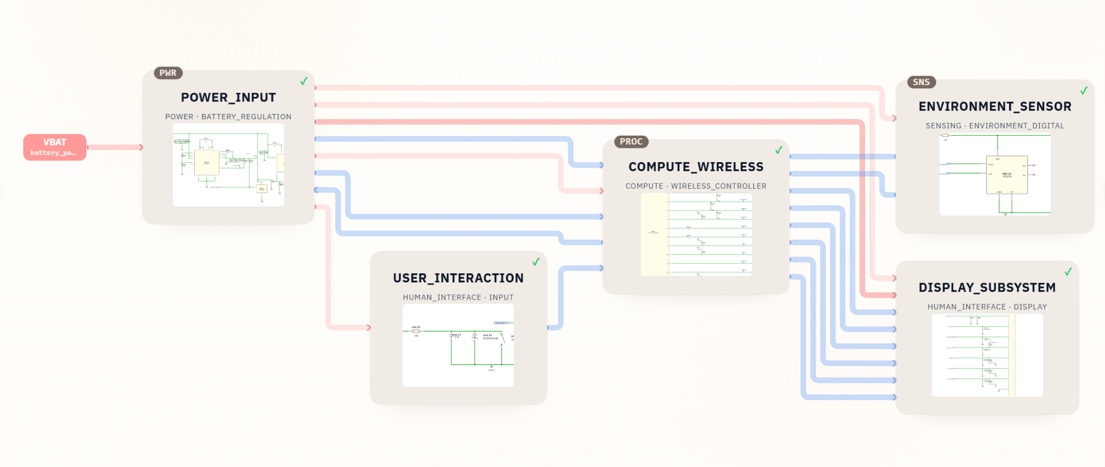
The real desktop robot ESP32 KiCad project uses an ESP32-WROOM-32E-N8 as its wireless controller. Its compute sheet provides a useful pin-planning example because it separates display outputs, an I2C sensor bus, and status inputs rather than treating every GPIO as interchangeable.
| GPIO | Project signal | Why the assignment is worth reviewing |
|---|---|---|
| GPIO32 | DISPLAY_BL_PWM |
Output-capable pin used for backlight PWM control |
| GPIO27 | DISPLAY_DC |
Digital display command/data selection |
| GPIO25 | DISPLAY_PWR_EN |
Output controls the display power path |
| GPIO26 | DISPLAY_RST_N |
Reset output needs a defined startup state |
| GPIO5 | DISPLAY_SPI_CS_N |
SPI chip select is also on a strapping pin, so its external bias must be checked |
| GPIO23 / GPIO18 | DISPLAY_SPI_MOSI / DISPLAY_SPI_SCK |
Conventional SPI outputs; no MISO is required for the shown one-way display path |
| GPIO21 / GPIO22 | I2C0_SDA / I2C0_SCL |
Common I2C mapping with external 3.3 kΩ pull-ups shown in the sheet |
| GPIO35 / GPIO34 | BATTERY_LOW_N / PGOOD_3V3 |
Input-only GPIOs are correctly used as status inputs rather than outputs |
| GPIO33 | UI_EVENT_N |
User-event input includes an external pull-up and capacitor for a defined hardware state |
This sheet is a generated first engineering draft, not a production reference design. It still needs review against the current module datasheet, display timing, peripheral power states, programming access, RF placement, firmware initialization, and the final PCB. The value of the example is that the assignments are visible and reviewable.
Common ESP32 Pinout Mistakes
- Copying a DevKit diagram into a module schematic. Board headers, module pins, and chip pads are different numbering systems.
- Assuming every ESP32 has the same GPIO set. ESP32, ESP32-C3, ESP32-S3, ESP32-S31, and other families differ in package, boot, USB, flash, and peripheral constraints.
- Driving 5 V into a module pin. A development board’s 5 V or VIN header does not make the ESP32 GPIO 5 V tolerant.
- Using GPIO34-39 as outputs. These pins are input-only on the classic ESP32, and they do not provide internal pull resistors.
- Choosing ADC2 for a measurement needed during Wi-Fi. Use ADC1 or explicitly design around the documented ADC2/Wi-Fi conflict.
- Loading a strapping pin during reset. Check resistor networks, peripheral output states, and capacitance before assuming a pin is free after boot.
- Treating default I2C or SPI pins as fixed. The GPIO matrix adds flexibility, but the final schematic and firmware must agree.
- Forgetting programming access. Keep UART0, GPIO0, and EN reachable unless a verified alternative is part of the product plan.
- Ignoring the antenna until layout. Reserve the module edge and keepout while the architecture is still flexible.
- Leaving unused inputs undefined. Use external or firmware-controlled pulls where the datasheet and power-state analysis require them.
How SpeedUp Fits
SpeedUp can turn a product prompt into an architecture, structured schematic sheets, a BOM, and an editable KiCad first draft. For an ESP32 device, that creates a concrete place to review the module choice, pin budget, power path, display or sensor buses, reset behavior, and named interfaces.
The generated output is a starting point for engineering review. A hardware engineer still validates the current Espressif documentation, component ratings, footprints, PCB placement, antenna constraints, firmware pin initialization, manufacturing access, safety, and compliance requirements before production.
Related ESP32 and Schematic Examples
- ESP32 e-ink MQTT display schematic — a separate ESP32-C3 project with Wi-Fi, power, and display interfaces.
- ESP32-S31 hardware design checklist — an example of why a newer ESP32 family needs its own pin and hardware review.
- How to review an AI-generated KiCad schematic — a wider workflow for checking generated first drafts.
FAQ
Do all ESP32 boards have the same pinout?
No. The ESP32 family contains multiple chips and modules, and development boards add another layer of header numbering and onboard circuitry. Match the exact chip, module suffix, board manufacturer, and board revision before assigning pins.
What is the difference between a 30-pin and 38-pin ESP32 board?
The numbers usually describe development-board header positions, not the internal ESP32 GPIO count. A 38-pin board may expose more module signals or power pins, while two boards with the same header count can still differ. Compare their board schematics and labels instead of choosing by pin count alone.
Can an ESP32 pin take 5 V?
Do not apply 5 V directly to ESP32-WROOM-32E GPIO or its 3V3 supply. Some development boards accept 5 V through a VIN or USB path because they include a regulator, but that is a board-level feature. Use an appropriate level shifter or divider when a peripheral signal exceeds the allowed GPIO voltage.
Which pins are I2C pins on a classic ESP32?
GPIO21 for SDA and GPIO22 for SCL are common defaults on a generic classic ESP32 setup. The GPIO matrix allows alternate pins in many cases, so confirm the firmware framework, choose output-capable pins where needed, and include correctly sized external pull-ups in the schematic.
Which ESP32 pins should not be used?
There is no universal “never use” list without knowing the exact part and circuit. Avoid module pins marked NC, do not assign output functions to GPIO34-39, protect strapping-pin states during reset, preserve flash or PSRAM connections, and account for programming, analog, and radio-related constraints.
Can I use GPIO0 as a normal output?
GPIO0 can operate as a GPIO after boot, but it is sampled to select boot mode during reset. Any external load or pull network must let it reach the required reset level and must not interfere with firmware download. A different output is often simpler when pins are available.
Start Your ESP32 Hardware Project
Turn your ESP32 pin and interface plan into an editable KiCad first draft.
Use SpeedUp to turn the product requirements into structured schematic sheets and an editable KiCad first draft for engineering review. Create a free account to begin.