
Quick Answer
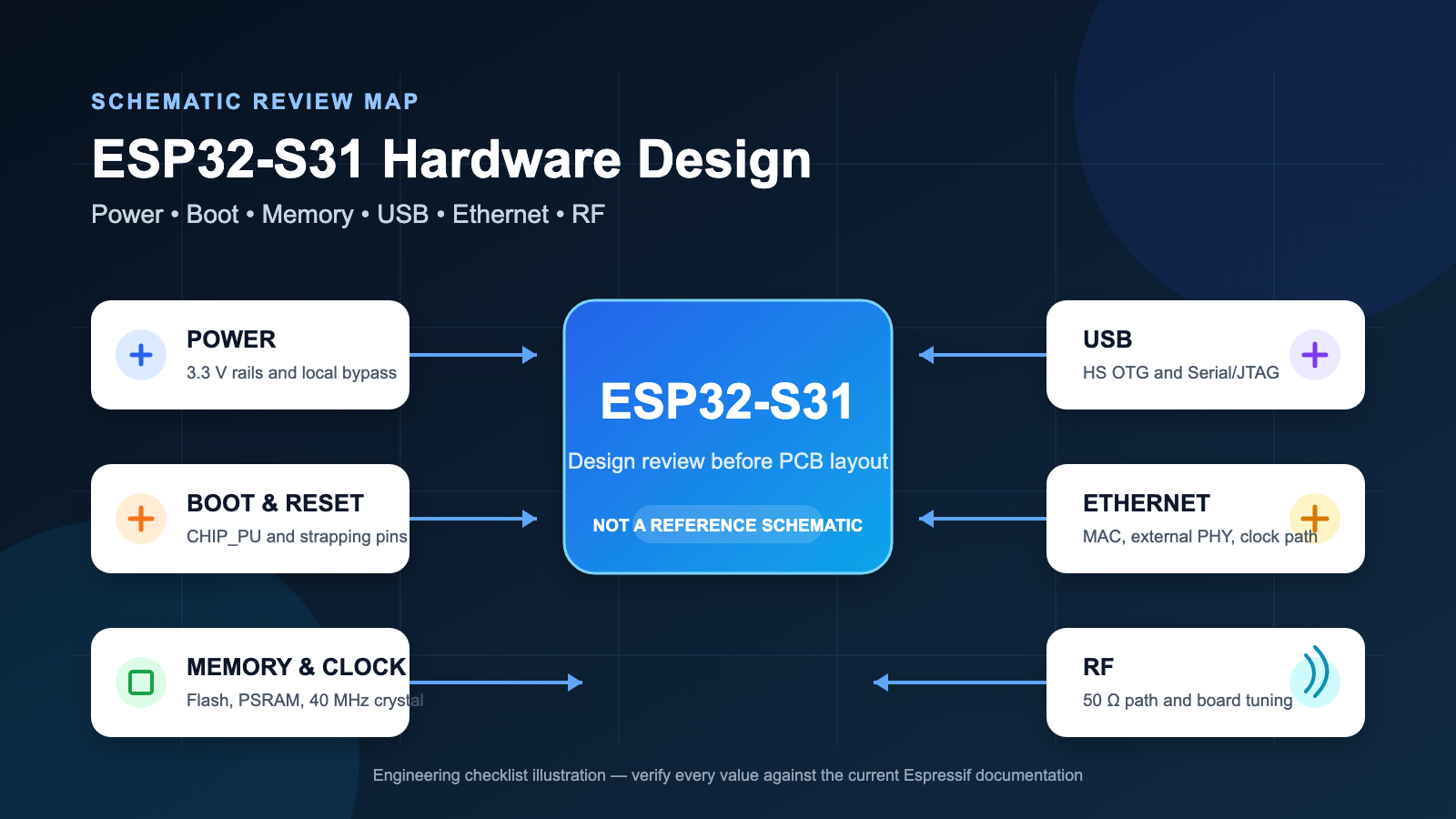
An ESP32-S31 schematic should be reviewed as a complete system, not as a copied MCU symbol. First decide whether the design uses an ESP32-S31 module or the bare SoC. Then verify every supply pin and local capacitor, CHIP_PU timing, boot-strapping states, external flash, the compulsory 40 MHz crystal, USB interfaces, Ethernet PHY connections, RF matching, and the final pin budget.
For a bare-chip design, Espressif currently recommends a 3.3 V supply capable of at least 800 mA, a defined CHIP_PU network, off-package NOR flash, and a 50 Ω RF path. The exact capacitor, inductor, matching, and pin choices depend on the package and PCB. If schedule and RF risk matter more than maximum integration, an ESP32-S31-WROOM module is usually the safer starting point.
What ESP32-S31 Adds
ESP32-S31 is Espressif’s high-performance connectivity SoC built around dual 32-bit RISC-V cores running at up to 320 MHz, with a low-power coprocessor, 512 KB of SRAM, and support for external high-speed PSRAM. Its integrated wireless set includes 2.4 GHz Wi-Fi 6, Bluetooth 5.4 LE and Classic, plus IEEE 802.15.4 for Zigbee and Thread. It also adds a Gigabit Ethernet MAC and high-speed USB capabilities. See the official ESP32-S31 product page and mass-production announcement for the current product summary.
Those features make the schematic more capable, but not automatically simpler. USB and Ethernet consume pins and add signal-integrity constraints. Multi-radio products need antenna, enclosure, coexistence, and certification planning. External memory adds another fast interface. The right first schematic is therefore a constrained architecture, not a symbol with every peripheral broken out.
First Decision: Module or Bare ESP32-S31?
| Decision area | ESP32-S31-WROOM module | Bare ESP32-S31 SoC |
|---|---|---|
| RF design | Module integrates the chip, crystal, memory, and RF implementation. Follow the module antenna keepout and placement rules. | You own the 50 Ω path, matching network, antenna or connector, layout tuning, and RF validation. |
| Memory and clock | Integrated according to the selected module variant. | External flash and the compulsory 40 MHz crystal must be designed and routed correctly. |
| PCB area and BOM | Larger module footprint, fewer RF and memory parts to source and validate. | Potentially smaller or more integrated product, with higher engineering and validation effort. |
| Best fit | Prototypes, lower-to-medium volumes, compressed schedules, and teams reducing RF risk. | High-volume or space-constrained products with experienced RF, layout, test, and compliance resources. |
Planning ESP32-S31 hardware?
Describe the package or module, power, boot, USB, Ethernet, memory, RF, connectors, and test requirements. Create a free account to start a reviewable, editable KiCad first draft.
Do not mix the two reference approaches. Module matching values and layout decisions are not a drop-in bare-chip RF design. Start from the documentation for the exact orderable part, including the ESP32-S31-WROOM-3 data sheet when using that module.
ESP32-S31 Schematic Review Checklist
| Block | Minimum review | Common failure |
|---|---|---|
| Power | 3.3 V current margin, all rail pins, local capacitors, RF rail filtering, startup behavior | Brownout or radio resets caused by supply droop and distant bypass parts |
| Reset | CHIP_PU never floating, correct RC or supervisor, rails stable before release | Intermittent boot during slow or noisy power ramps |
| Boot and programming | GPIO37/60/61 straps, download mode access, UART0 or USB debug path | External loads force the wrong boot mode |
| Memory | Validated NOR flash, supported mode, rail voltage, optional series footprints, short routing | Unqualified flash or copied high-speed routing fails across temperature |
| Clock | 40 MHz crystal, load-cap calculation, required series inductor, optional 32.768 kHz path | Crystal starts in the lab but misses frequency or startup margin |
| USB | Choose HS OTG versus Serial/JTAG, connector CC network, ESD, controlled routing, VBUS behavior | USB-C power works but data or programming does not |
| Ethernet | External PHY, interface mode, reference clock direction, strap states, magnetics and ESD | Treating the internal MAC as a complete Ethernet port |
| RF | 50 Ω trace, matching footprints, antenna keepout, enclosure and tuning plan | Copying another board’s matching values without tuning this PCB |
| GPIO plan | Package pinout, straps, dedicated interfaces, voltage domains, startup states, test access | Discovering after layout that two required functions need the same pin |
Use this as a review index, then check the current Espressif ESP32-S31 schematic checklist and ESP32-S31 data sheet for exact limits and package pin assignments.
Power Supply and Decoupling
Espressif recommends a single 3.3 V supply with at least 800 mA available for a bare ESP32-S31 design. That rating is a starting point for the SoC, not a complete product power budget. Add display, Ethernet PHY, sensors, USB peripherals, external memory, LEDs, relays, and peak radio activity before selecting the regulator. Review input-source tolerance, thermal dissipation, startup ramp, transient response, brownout behavior, and the real battery or USB current limit.
Each supply group needs the capacitors shown in the current hardware guide placed close to its pins with a short return path. The main power entry should include ESD protection and at least 10 µF of bulk capacitance. VDDPST_1 uses local 0.1 µF and 1 µF bypassing; the analog and RF supply groups have their own local networks. Espressif highlights VDDA3 and VDDA4 because RF bursts create fast current demand, and recommends an LC-filtered path with an inductor rated for at least 500 mA.
Treat those values as net-specific requirements, not one generic “decoupling bank.” Verify the exact pins and latest values for the selected package, then apply the decoupling capacitor value and PCB placement checklist before layout.
CHIP_PU, Reset, and Boot-Strapping Pins
CHIP_PU enables the chip when HIGH and resets it when LOW. It must never float. The supply rails need to be stable before CHIP_PU rises; the current Espressif guide specifies at least 1 ms for both power stabilization and reset-low time. A 10 kΩ pull-up with 1 µF to ground is the initial RC recommendation. When the source ramps slowly, dips during startup, or can cycle unpredictably, reserve a reset supervisor with an appropriate threshold instead of expecting one RC pair to fix every waveform.
GPIO37, GPIO60, and GPIO61 are strapping pins. GPIO60 and GPIO61 participate in boot-mode selection; the normal SPI boot condition and download-mode condition must match the latest table. Espressif recommends a pull-up on GPIO61 and warns against a high-value capacitor there. Audit every peripheral, level shifter, connector, and test jig attached to a strap pin. A device that is high impedance after boot can still force the wrong level during reset.
Also make programming and recovery deliberate. UART0 uses GPIO58 and GPIO59 by default for downloads and logs, with a 499 Ω series resistor recommended on U0TXD. If the product relies on USB Serial/JTAG instead, retain accessible pads or a connector strategy that works when the main application firmware is broken.
Flash, PSRAM, and Clock Design
A bare ESP32-S31 requires off-package NOR flash for the current firmware flow. Confirm the supported interface mode, flash voltage, capacity, package, temperature grade, and exact part against the current qualified list. Espressif’s guidance allows SPI, dual, and quad modes and describes capacities up to 256 MB. Reserve zero-ohm series-resistor footprints on fast flash signals so bring-up can tune edges without cutting traces.
Some variants integrate octal 1.8 V PSRAM inside the package; those internal PSRAM pins are not bonded out for reuse. For any external high-speed memory, follow the package-specific pin and routing guidance and validate the supported ESP-IDF configuration before committing the BOM.
The 40 MHz crystal is compulsory for the bare-chip design and should meet the current ±10 ppm accuracy requirement. The published checklist calls for a 24 nH, 0201 series inductor on XTAL_P even when RF is not used. Calculate the initial load capacitors from the crystal load specification and measured stray capacitance, then verify startup and frequency on the assembled PCB. If the optional 32.768 kHz crystal is used, check its ESR and reserve the bias-resistor footprint described by Espressif.
USB-C, High-Speed USB, and Serial/JTAG
ESP32-S31 exposes separate high-speed USB OTG and USB Serial/JTAG paths. Decide which interface powers the board, programs it, carries product data, or supports host/device operation. Then trace each connector pin to the intended controller pins; a board can enumerate on one interface while the recovery workflow expects the other.
For USB Serial/JTAG, Espressif recommends reserving 22 Ω or 33 Ω series resistors and optional shunt-capacitor footprints close to the chip for signal tuning. The complete USB-C design also needs correct CC resistors for the chosen power role, ESD protection with a short return, VBUS sensing and power-path behavior, controlled differential routing, connector orientation, shield treatment, and no accidental back-power path. Use the USB-C schematic checklist before PCB layout for that connector-level review.
Gigabit Ethernet MAC and External PHY
The ESP32-S31 includes an Ethernet MAC, not the analog PHY, magnetics, connector, protection, and termination required for a physical network port. Select a supported external PHY and one interface mode—MII, RMII, or RGMII—then confirm pin availability, IO voltage, clock direction, reset timing, strap resistors, MDIO/MDC management, and the PHY’s own power rails.
Clock topology deserves an explicit diagram. The hardware guide recommends a series footprint on the clock signal for tuning. In RMII, GPIO13 is a clock input; designs needing an output clock use the specified alternative clock pad and connection scheme. Do not infer direction from a signal name. Follow the exact current table for the selected interface and route the high-speed group according to both SoC and PHY requirements.
At the connector side, review magnetics, chassis and digital ground strategy, common-mode protection, ESD discharge path, center-tap power, PoE requirements if any, and differential-pair constraints. Ethernet is a subsystem, not one MAC-to-RJ45 net bundle.
RF Matching, Antenna, and PCB Layout
For the bare SoC, route the RF signal as a controlled 50 Ω transmission line. Place the matching network immediately next to the chip, preserve at least two configurable CLC sections, and use the component size recommended in the current guideline. Espressif suggests a CLCCL arrangement near the SoC and another CLC section near the antenna. Initial values are not final values: stackup, ground shape, enclosure, battery, display, cable, antenna, and assembly tolerances all change the measured impedance.
Do not copy module matching values onto a custom bare-chip board. Reserve tuning footprints, control the ground and keepout geometry, prevent digital traces from crossing the RF return path, and plan conducted and radiated test access. A module can reduce this risk, but the carrier PCB still has to respect its antenna keepout, edge placement, ground clearance, enclosure materials, and certification conditions.
GPIO and Peripheral Pin Planning
ESP32-S31 offers up to 60 GPIOs, but “up to” is not the number freely available to your design. Package selection, boot straps, UART0, memory, USB, Ethernet mode, crystal pins, RF, power domains, debug access, touch or display functions, and internal package options all reduce or constrain the usable set.
- Lock the exact package or module variant and import the matching official pin table.
- Allocate non-negotiable functions first: supplies, grounds, RF, clocks, memory, straps, reset, programming, USB, and Ethernet.
- Record every pin’s reset state, pull state, voltage domain, and board-level load.
- Assign flexible buses and GPIO only after the fixed functions are conflict-free.
- Reserve test access for power rails, reset, boot, debug, USB, Ethernet clocks, and RF where appropriate.
- Run a final pin audit against the latest data sheet and selected ESP-IDF peripheral configuration.
A Real SpeedUp Example: System-Level ESP32 Review
The existing ESP32 E-Ink MQTT display schematic example uses an earlier ESP32 family device, not ESP32-S31, so it is not a pin-compatible reference design. It is useful here for a different reason: the generated project separates power, MCU, display, buttons, LEDs, and connectors into reviewable sheets instead of hiding the product behind one block.

For an ESP32-S31 product, that same decomposition should expose the additional high-risk blocks: every supply group, CHIP_PU and straps, flash and PSRAM, 40 MHz clock, the selected USB paths, external Ethernet PHY, RF section, and a pin-allocation table. The structure makes review faster; it does not eliminate engineering verification.
ESP32-S31 vs ESP32-S3 for New Designs
ESP32-S31 is not simply a faster ESP32-S3. According to Espressif’s official ESP32-S31 FAQ, S31 moves to dual RISC-V application cores up to 320 MHz and adds Wi-Fi 6, IEEE 802.15.4 for Zigbee and Thread, Bluetooth Classic alongside BLE, Gigabit Ethernet MAC, high-speed USB, and new accelerators. These additions can consolidate a connected product that would otherwise need more companion ICs.
Choose S31 when its connectivity, compute, memory, or interface set materially improves the product architecture and the newer platform fits your software and supply plan. Choose S3 when its mature ecosystem, existing firmware, qualified modules, known RF path, and adequate performance reduce schedule and lifecycle risk. The schematic decision should include SDK readiness, module availability, certifications, power, package, memory, board complexity, and the team’s ability to validate a new platform—not just headline clock rate.
Common ESP32-S31 Hardware Design Mistakes
- Using a generic ESP32 symbol or an ESP32-S3 reference design as if the ESP32-S31 pinout and power network were interchangeable.
- Selecting the package after GPIO assignment, then discovering conflicts with fixed interfaces and strapping pins.
- Sizing the regulator for average current while ignoring radio, USB, Ethernet, display, and external-memory transients.
- Letting CHIP_PU float or relying on an RC reset network without checking the actual supply ramp.
- Attaching LEDs, level shifters, or peripherals to boot straps without analyzing their reset-time state.
- Choosing flash or PSRAM by capacity alone without validating interface, voltage, timing, and software support.
- Treating USB-C, Ethernet, or RF as schematic-only interfaces and postponing return-path and impedance decisions until layout.
- Copying RF matching values from a development board or module onto a different stackup and antenna geometry.
- Freezing the design against a preliminary document without a revision and errata check.
How SpeedUp Fits
SpeedUp can turn an ESP32-S31 product requirement into a structured KiCad schematic draft with explicit power, reset, boot, memory, USB, Ethernet, RF, connector, and test-point sheets. That gives an engineer a concrete design to review against the official data sheet instead of starting from an empty canvas or an unrelated reference board.
The generated schematic is an engineering draft, not a production-ready Espressif reference design. The engineer still selects the exact orderable part, replaces provisional symbols or footprints, validates every limit and approved component, completes PCB stackup and high-speed/RF layout, tests hardware, qualifies sourcing, and finishes safety, EMC, radio, and manufacturing compliance. The AI-generated KiCad schematic review guide provides the broader review workflow.
Related SpeedUp Guides
- KiCad schematic checklist before PCB layout — validate constraints, footprints, return paths, placement, and fabrication readiness after the circuit review.
- Use the official ESP32-S31 ESP-IDF getting-started guide to confirm the current toolchain, target support, programming flow, and example projects.
- Review the official ESP32-S31 Function CoreBoard user guide for a module-based evaluation platform and bring-up reference.
FAQ
What power supply does ESP32-S31 need?
For a bare SoC, Espressif currently recommends a 3.3 V supply with at least 800 mA available. The final regulator must also support all other loads and real transient, thermal, startup, and source conditions. A module design must follow the exact module data sheet.
Does ESP32-S31 need external flash?
A bare ESP32-S31 uses off-package NOR flash for the current firmware flow. Some module or package variants integrate memory, so check the exact orderable part. Validate the flash model, voltage, interface mode, capacity, routing, and current ESP-IDF support.
Does ESP32-S31 have Ethernet?
It includes a Gigabit Ethernet MAC. A physical Ethernet port still needs an external PHY plus its power, reference clock, straps, management interface, magnetics, connector, protection, and PCB layout.
Does ESP32-S31 support Zigbee and Thread?
Yes. ESP32-S31 integrates IEEE 802.15.4 alongside 2.4 GHz Wi-Fi 6 and Bluetooth 5.4, enabling Zigbee, Thread, and Matter-related architectures subject to the current software stack and certification requirements.
Can I copy an ESP32-S3 schematic for ESP32-S31?
No. It can help identify product-level blocks, but the pinout, power groups, boot straps, memory, clocks, USB, Ethernet, RF network, package, and software target must be rebuilt or verified from the ESP32-S31 documentation.
Should I use an ESP32-S31 module or the bare chip?
Use a module when schedule, RF risk, lower engineering effort, and easier prototyping dominate. Consider the bare chip when volume, PCB area, integration, or custom antenna requirements justify the added memory, clock, RF, layout, test, sourcing, and certification work.
Is the ESP32-S31 data sheet final?
The public data sheet reviewed for this article is marked preliminary even though Espressif has announced mass production. Check the current revision, errata, hardware guidelines, module documentation, and ESP-IDF release notes immediately before design freeze.
Start Your ESP32-S31 Project
Turn your ESP32-S31 hardware plan into a structured, editable KiCad first draft.
Use SpeedUp to turn the product requirements into structured schematic sheets and an editable KiCad first draft for engineering review. Create a free account to begin.
Comments
No comments yet.
Leave a Reply