
Quick Answer
A schematic review checklist for an AI-generated KiCad project should start with the product requirement, then check the architecture, power tree, MCU assumptions, interfaces, storage, RF, BOM, footprints, and production risks. Do not treat the generated schematic as a finished reference design. Treat it as a first engineering draft that should make review faster by giving you concrete nets, modules, part choices, and documentation to inspect.
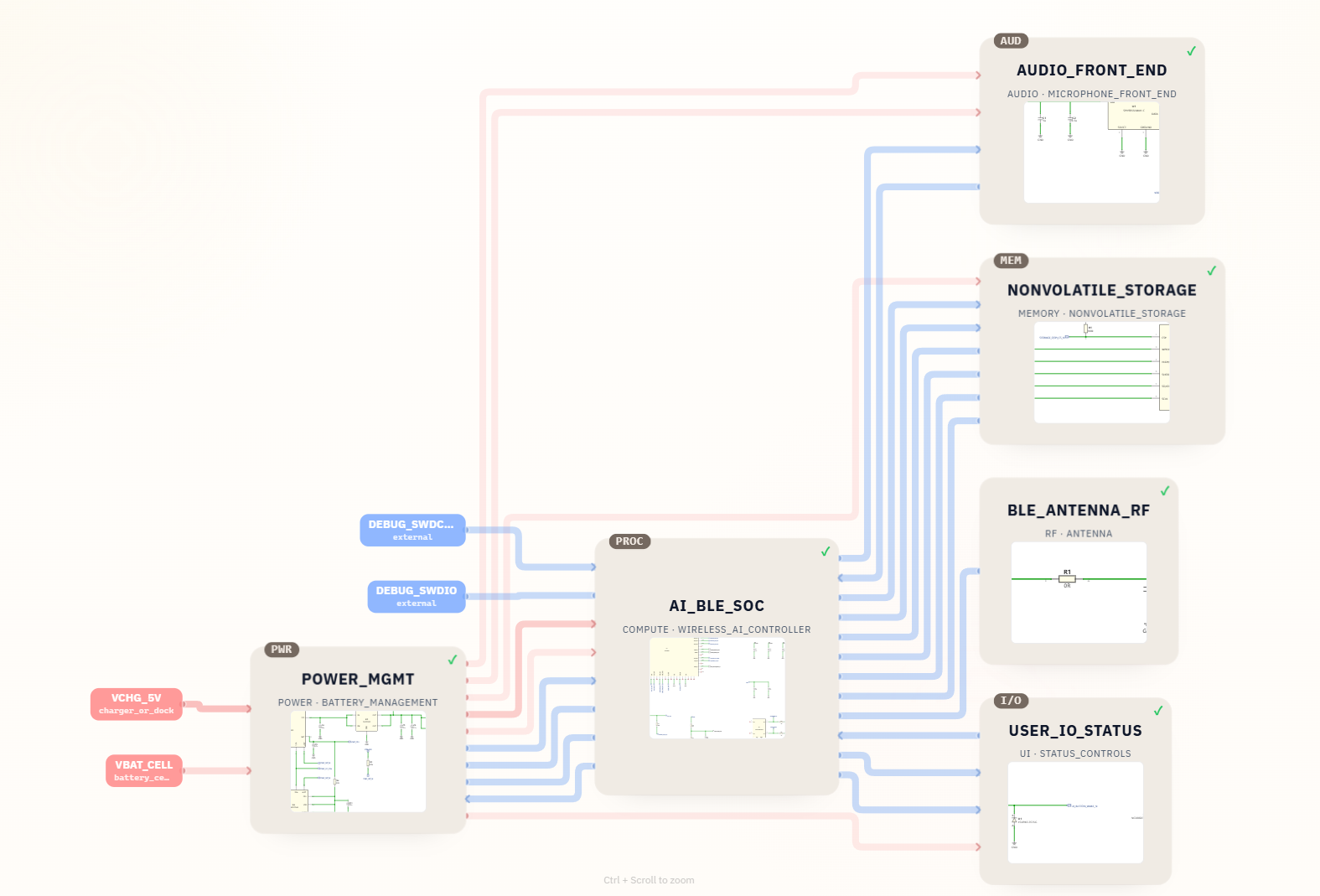
The most useful review order is: block diagram first, top-level schematic second, subsystem sheets third, BOM and footprints fourth, then firmware, layout, sourcing, and compliance assumptions. The example below uses a SpeedUp-generated AI recorder project with BLE sync, PDM audio capture, QSPI storage, battery power management, and RF antenna circuitry. It shows how an AI schematic generator can create a reviewable starting point, while also showing exactly where human engineering review still matters.
Why This Matters
AI schematic generators are useful because they can turn a product idea into a structured hardware draft quickly. But hardware failure modes are still physical. A plausible-looking schematic can hide weak power sequencing, mismatched footprints, missing debug access, noisy analog supply routing, RF antenna constraints, unavailable parts, or firmware assumptions that are never stated clearly.
That is why the right question is not "did AI generate a schematic?" The better question is "did the generated KiCad project expose the design decisions clearly enough for an engineer to review them?" A good AI-generated schematic should be organized into meaningful blocks, use named nets, include a BOM, and make subsystem boundaries easy to inspect.
Schematic Review Checklist
| Review area | What to check | Example in the SpeedUp project |
|---|---|---|
| Product requirement | Confirm the schematic matches the device goal, size, power source, wireless behavior, and sensing or audio task. | Tiny magnetic AI label microphone for continuous voice recording, real-time transcription, and BLE phone sync. |
| Architecture | Verify that blocks are separated in a way engineers can review. | POWER_MGMT, AI_BLE_SOC, AUDIO_FRONT_END, NONVOLATILE_STORAGE, BLE_ANTENNA_RF, and USER_IO_STATUS. |
| Power tree | Check charger, battery path, rails, load switching, fuel gauge, and sleep-current assumptions. | BQ21080YBGR, DIO7005HCST5, ST1PS01DJR, and MAX17048X+T10 appear in the generated BOM. |
| MCU and firmware | Review boot, debug, secure update, pin mapping, sleep states, and bus ownership. | NRF52840-QIAA-F-R7 is marked as the BLE/audio controller, with notes about secure boot, signed DFU, and debug lock. |
| Audio path | Check microphone supply filtering, PDM clock/data routing, decoupling, and footprint accuracy. | SPH9855LM4H-C is used as a digital PDM MEMS microphone, with a note to verify the mechanical land pattern. |
| Storage | Confirm memory interface, supply voltage, retention, endurance, and firmware behavior. | GD5F1GQ5REYIGR QSPI NAND is listed with 1 Gbit capacity, ECC, endurance, and retention notes. |
| RF and antenna | Check antenna matching, keepout, enclosure effects, and tuning placeholders. | 2450AT18A100E chip antenna includes notes about enclosure revalidation and vendor keepout guidance. |
| BOM and footprints | Compare MPNs, package names, footprints, DNP/tuning parts, and sourcing risk. | The ZIP includes a BOM with 50 line items and 87 placed quantities plus local symbol and footprint files. |
Need a concrete schematic before engineering review?
Describe the product behavior, architecture, power sources, interfaces, components, connectors, and constraints. Create a free account to start a reviewable, editable KiCad first draft.
1. Requirements and Architecture Review
Start by comparing the schematic against the product requirement. Confirm the power source, operating states, main interfaces, sensors, radios, connectors, user controls, programming method, size constraints, and expected outputs. A technically neat schematic can still be wrong if it implements the wrong product behavior.
Then inspect the block diagram and top-level hierarchy. Every major function should have a clear owner, supply rail, interface, and review boundary. Check that the top-level sheets match the block diagram, named nets cross sheets consistently, and no required function exists only in prose.
- Trace every product requirement to a schematic block or an explicit unresolved item.
- Confirm input, output, power, communication, programming, and test interfaces.
- Identify assumptions that belong to firmware, PCB layout, enclosure, sourcing, or compliance.
- Stop detailed review if the architecture does not match the intended device.
Example From a Real SpeedUp Project
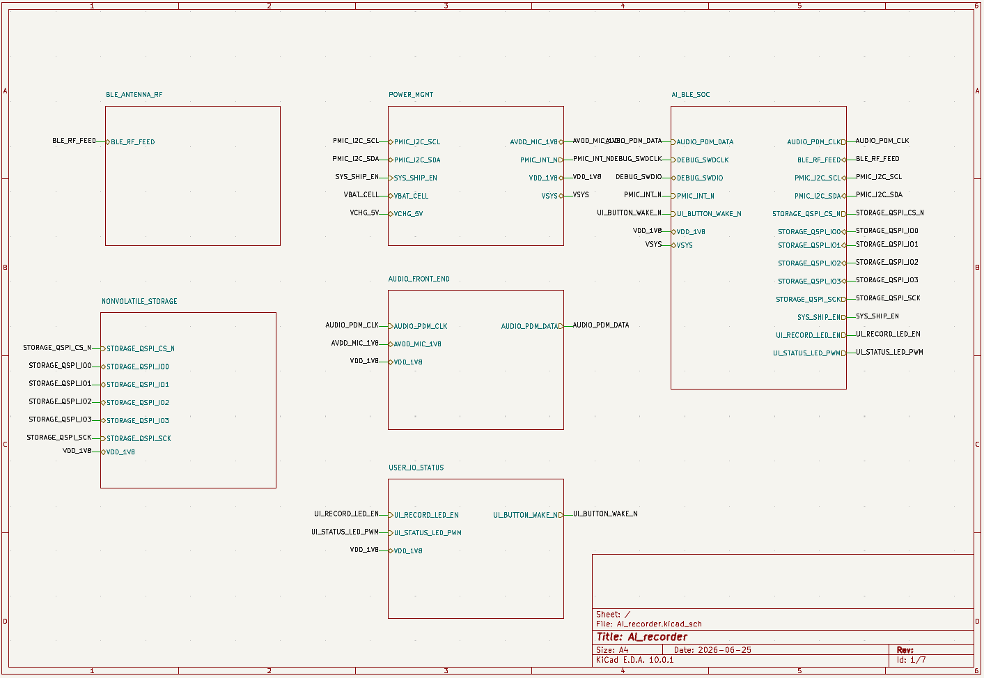
This guide uses the magnetic AI label microphone KiCad project as the running example. The original prompt asked for a tiny magnetic AI label microphone that records continuously, supports real-time transcription, and syncs to a phone over BLE.
That is a demanding prompt because it mixes power, audio, storage, wireless, mechanical, and firmware concerns. The generated KiCad project is therefore useful for review because it does not collapse everything into one schematic sheet. It separates the design into subsystem sheets and gives the reviewer named signals such as AUDIO_PDM_CLK, AUDIO_PDM_DATA, STORAGE_QSPI_*, PMIC_I2C_*, BLE_RF_FEED, VSYS, and VDD_1V8.
2. Power Tree, Charging, and Protection Review
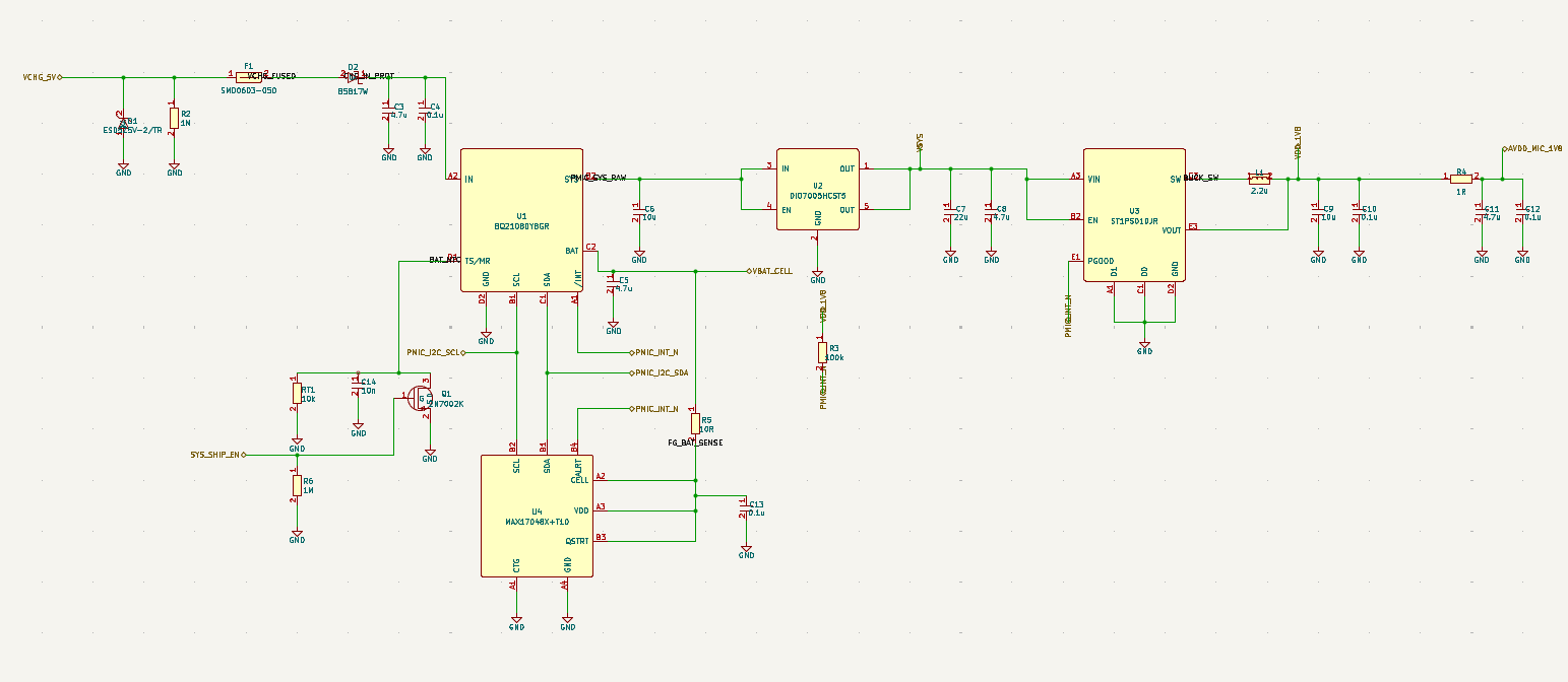
Power review should come before detailed peripheral review. In the AI recorder example, the BOM includes a BQ21080YBGR 1-cell Li-ion charger and SYS power-path controller, a DIO7005HCST5 VSYS load switch, a ST1PS01DJR 1.8 V buck regulator, and a MAX17048X+T10 fuel gauge.
Those parts give the schematic a credible battery-powered structure, but they also create review questions. Is the charge current appropriate for the chosen cell? Are thermal limits acceptable in a small magnetic enclosure? Does the load switch support the expected recorder burst current? Does the 1.8 V rail cover the BLE SoC, memory, microphone, and UI needs? Is the fuel gauge connected in a way firmware can actually use?
For AI-generated schematics, the power sheet should make these questions easy to ask. It does not need to answer every production detail on the first pass, but it should expose the rails, control pins, protection parts, bypass capacitors, and power-state assumptions.
3. MCU, Clocks, Debug, Firmware, and Security Review
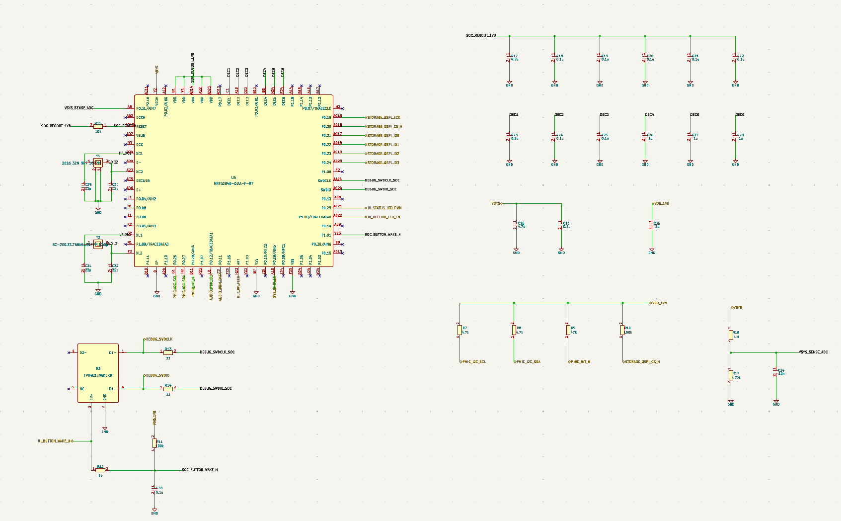
The AI recorder example uses NRF52840-QIAA-F-R7 as the BLE/audio controller. The BOM note calls out secure boot, signed DFU, and production debug lock. That is a good sign because BLE audio or recorder devices often become firmware-heavy products, not just electrical designs.
When reviewing this section, check that the generated schematic has a believable firmware path. Look for SWD or debug access, reset behavior, clock sources, RF feed, audio pins, storage bus pins, PMIC interrupt lines, and wake or record controls. If the design expects secure firmware updates or phone sync, the schematic should not ignore production debug lock, bootloader strategy, storage encryption, or manufacturing test hooks.
Audio, Storage, And RF Review
The audio path in the example uses a digital PDM MEMS microphone, SPH9855LM4H-C. The BOM also notes that the selected part search result did not provide an explicit footprint and that the mechanical land pattern needs verification before layout. That is exactly the kind of warning that should survive from generated output into human review.
For storage, the project uses GD5F1GQ5REYIGR QSPI NAND, with BOM notes for 1 Gbit capacity, ECC, endurance, retention, standby current, and supply voltage. That turns storage review into a concrete checklist: voltage compatibility, bus pins, boot-time state, file system strategy, write endurance, and how much local audio buffering is realistic.
For RF, the design includes a 2450AT18A100E 2.4 GHz chip antenna and tuning placeholders. The BOM note says the final antenna choice and matching must be revalidated in the magnetic label enclosure, with keepout required per vendor guidance. This is a good reminder that an AI-generated RF schematic is not enough. The enclosure, board stackup, ground clearance, nearby metal, and final tuning still decide wireless performance.
4. Interfaces, Connectors, Symbols, Footprints, and ERC
Review each interface end to end rather than checking isolated components. Confirm voltage levels, direction, pullups or pulldowns, termination, ESD protection, connector pinout, shield and ground strategy, bus ownership, and what happens during reset or when one side is unpowered.
Next, validate symbols and footprints against current manufacturer documentation. Check hidden power pins, multi-unit symbols, exposed pads, pin-one orientation, package suffixes, mechanical outlines, connector mating direction, and whether the selected footprint actually matches the orderable part in the BOM.
Run KiCad ERC, but do not treat a clean report as approval. Review every waived warning, unconnected pin, power-input warning, no-connect flag, duplicated net name, and hierarchical connection manually. ERC checks rule consistency; it does not prove that the architecture, component values, interfaces, or safety decisions are correct.
- Verify USB-C, I2C, SPI, UART, CAN, SWD, analog, and RF interfaces against their electrical requirements.
- Confirm connector numbering from the mating side and document unused pins.
- Match manufacturer part number, symbol, package, footprint, and 3D/mechanical constraints.
- Record every ERC waiver with a reason that another reviewer can understand.
5. BOM, Sourcing, and Lifecycle Review
| BOM area | Example parts in this project | Review before production |
|---|---|---|
| Battery and power path | BQ21080YBGR, DIO7005HCST5, ST1PS01DJR, MAX17048X+T10 |
Confirm charge current, rail sequencing, quiescent current, thermal limits, and battery assumptions. |
| BLE and compute | NRF52840-QIAA-F-R7 |
Confirm firmware capacity, RF layout requirements, debug access, secure boot, signed DFU, and production lock settings. |
| Audio input | SPH9855LM4H-C |
Verify microphone footprint, acoustic port, PDM routing, supply filtering, and enclosure opening. |
| Local storage | GD5F1GQ5REYIGR |
Check QSPI bus wiring, voltage, endurance, retention, firmware storage format, and write-failure handling. |
| RF antenna | 2450AT18A100E |
Validate matching, keepout, enclosure effects, placement, test plan, and certification risk. |
The generated BOM has 50 line items and 87 placed quantities. That is enough to make review concrete. Instead of arguing over a concept, engineers can inspect actual MPNs, footprints, notes, tuning placeholders, and subsystem dependencies.
6. PCB Layout Handoff and Sign-Off
A schematic is ready to hand off to PCB layout only when the unresolved electrical decisions are visible and assigned. The handoff should include validated footprints, placement constraints, controlled-impedance requirements, antenna and sensor keepouts, current-carrying paths, thermal concerns, connector access, test points, programming access, safety spacing, and any components that require tuning after prototypes arrive.
| Sign-off gate | Evidence required before layout |
|---|---|
| Requirements | Every required function is implemented or explicitly marked unresolved. |
| Electrical review | Power, interfaces, reset, clocks, protection, analog, and RF paths have named reviewers. |
| Library validation | Symbols and footprints match the exact manufacturer parts and package variants. |
| ERC and open issues | ERC warnings are resolved or documented; remaining issues have owners and deadlines. |
| Layout constraints | Keepouts, impedance, current, thermal, mechanical, test, and safety constraints are transferred to layout. |
| Production boundary | The team agrees that layout handoff is not manufacturing approval; prototype validation, compliance, DFM, and test planning remain. |
Common Mistakes
- Reviewing only the block diagram and skipping the generated KiCad sheets.
- Treating a plausible BOM as a validated sourcing plan.
- Ignoring footprint warnings, especially for microphones, antennas, wafer-level packages, and tiny power ICs.
- Forgetting that BLE, audio recording, local storage, and battery life are firmware problems as much as schematic problems.
- Assuming RF antenna performance from a schematic without enclosure, keepout, matching, and test data.
- Publishing or manufacturing from an AI-generated first draft without electrical, layout, firmware, compliance, and DFM review.
How SpeedUp Fits
SpeedUp helps by moving the first pass from a blank page to a reviewable engineering draft. A prompt can become a block diagram, schematic hierarchy, BOM, and editable KiCad project files. That makes the next discussion more specific: reviewers can point to rails, nets, modules, components, footprints, and missing validation work.
The right workflow is not to skip engineering review. The better workflow is to use generated schematics to start review earlier. Engineers still decide whether the power architecture is safe, whether footprints are right, whether RF can pass real tests, whether firmware can support the product behavior, and whether the design is ready for layout and manufacturing.
Detailed Checklists and Real Project Evidence
Use this page as the overall review framework, then open the most relevant detailed checklist or project example for the subsystem you are reviewing.
Detailed schematic checklists
- AI-generated KiCad schematic checklist before PCB layout — final handoff checks after schematic review.
- Battery-powered sensor circuit design checklist — charging, regulation, sleep current, sensing, and display risks.
- MCP73831 charger circuit schematic checklist — charge current, thermal behavior, battery safety, and status pins.
- BME280 KiCad and I2C sensor checklist — supply, pullups, addressing, filtering, and placement.
- SN65HVD230 CAN bus schematic checklist — termination, protection, transceiver supply, and connector review.
- CAN bus termination resistor placement and testing — 120-ohm endpoint placement, split termination, selectable termination, and powered-off resistance checks.
- Flyback diode polarity, placement, and sizing guide — inductive clamp checks for relays, solenoids, and brushed-motor outputs.
- Solder jumpers in KiCad schematics — configuration, isolation, debug, and production-default review.
Real SpeedUp project evidence
- Magnetic AI label microphone KiCad project — the power, BLE, audio, storage, and RF example used throughout this guide.
- nRF54L15 KiCad schematic project — provisional symbol, RF, USB debug, power, and BOM review.
- Temperature and humidity sensor KiCad project — USB-C charging, I2C sensing, display, and low-power review.
- ESP32 e-ink MQTT display project — connected display, MCU, interface, power, and firmware assumptions.
FAQ
Can an AI schematic generator create a useful KiCad project?
Yes, it can create a useful first draft when the output includes a block diagram, schematic sheets, BOM, symbols, footprints, and named interfaces. It still needs engineering review before layout or production.
What should I check first in an AI-generated schematic?
Start with the product requirement and architecture, then review power, MCU, interfaces, BOM, and footprints. If the block diagram and top-level schematic do not match the product goal, detailed subsystem review will not fix the design.
Is a generated KiCad schematic production-ready?
No. Treat it as a review starting point. Production readiness requires electrical validation, footprint checks, layout constraints, firmware validation, sourcing review, enclosure review, and any safety or RF compliance work.
Why does BOM review matter for AI-generated hardware?
BOM review exposes whether the design uses real parts, correct packages, available footprints, realistic values, and documented caveats. It also reveals risks such as generic passives, unavailable parts, and footprint warnings.
What should be reviewed before PCB layout starts?
Before PCB layout, confirm requirements, power rails, protection, clocks, reset, programming access, interfaces, connector pinouts, symbols, footprints, ERC results, BOM status, test points, RF and analog constraints, mechanical keepouts, and safety spacing. Any unresolved item should have an owner and should be visible to the PCB designer.
Does a clean KiCad ERC mean the schematic is correct?
No. ERC can identify rule and connectivity problems, but it cannot prove that the product architecture, component values, footprint choices, interface behavior, power budget, RF implementation, or safety decisions are correct. Treat ERC as one review input, not final approval.
Start With an Editable Schematic Draft
Turn your product brief into structured schematic sheets that engineers can inspect and refine.
Use SpeedUp to turn the product requirements into structured schematic sheets and an editable KiCad first draft for engineering review. Create a free account to begin.
Comments
No comments yet.
Leave a Reply