
Quick Answer
An I2C pull-up resistor cannot be chosen from bus speed alone. Start by calculating a minimum resistance from the supply voltage, the maximum valid LOW voltage, and the weakest device’s sink-current capability. Then calculate a maximum resistance from the allowed rise time and the total bus capacitance. Choose a standard value between those limits and verify the real SDA and SCL rise times on the assembled board.
A 4.7 kΩ resistor is a common starting point for a short 3.3 V, 100 kHz bus, but it is not a universal answer. A 400 kHz bus with 200 pF of capacitance may need a value around 1 kΩ to 1.8 kΩ, while a short low-capacitance bus may work with a larger value. Also count every pull-up already fitted on sensor modules, displays, level shifters, and development boards because parallel resistors reduce the effective resistance.
Why I2C Needs Pull-Up Resistors
I2C devices normally use open-drain or open-collector outputs on SDA and SCL. A device can pull a line LOW, but it does not actively drive the line HIGH. A pull-up resistor returns the line to the bus supply when every connected device releases it. This wired-AND behavior lets multiple devices share the same two signals and supports arbitration and clock stretching.
The resistor creates an engineering trade-off. A smaller resistance charges the bus capacitance faster and produces a sharper rising edge, but it also requires more sink current whenever the line is LOW. A larger resistance reduces LOW-state current but produces a slower edge. If the edge does not reach a valid HIGH before the next transition, the bus can produce intermittent acknowledgments, corrupted transfers, or failures that appear only with certain cables, temperatures, probes, or device combinations.
I2C Pull-Up Resistor Calculator Formulas
The official NXP I2C-bus specification and TI pull-up resistor calculation note define the same two boundaries.
Maximum resistance from rise time
Rp(max) = tr(max) / (0.8473 × Cb)tr(max)is the maximum permitted rise time for the selected I2C mode.Cbis the total capacitance on one bus line, including device pins, PCB traces, connectors, cables, level shifters, and measurement probes.- The factor
0.8473comes from the time required for an RC waveform to rise from 30% to 70% of the bus voltage.
Minimum resistance from sink current
Rp(min) = (VDD - VOL(max)) / IOLVOL(max) and IOL must come from the bus specification and the data sheets for the actual controller, targets, level shifters, and buffers. The weakest device on the bus sets the practical limit. Do not assume every device can sink the Fast-mode Plus current simply because the controller supports a 1 MHz clock.
Rise-Time Limits and Calculated Maximum Values
NXP specifies different maximum rise times for the common I2C modes. The table below also shows the maximum pull-up resistance calculated for several estimated bus capacitances. These are mathematical upper limits, not automatic production choices.
| Mode | Nominal maximum rate | Maximum rise time | Rp(max) at 50 pF | Rp(max) at 100 pF | Rp(max) at 200 pF |
|---|---|---|---|---|---|
| Standard-mode | 100 kbit/s | 1000 ns | 23.6 kΩ | 11.8 kΩ | 5.90 kΩ |
| Fast-mode | 400 kbit/s | 300 ns | 7.08 kΩ | 3.54 kΩ | 1.77 kΩ |
| Fast-mode Plus | 1 Mbit/s | 120 ns | 2.83 kΩ | 1.42 kΩ | 0.71 kΩ |
Designing a shared I2C sensor bus?
Describe the bus voltage, devices, capacitance, speed, powered-off behavior, interrupt lines, and low-power target. Create a free account to start a reviewable, editable KiCad first draft.
At 400 pF, the calculated Fast-mode maximum is about 0.89 kΩ. A 3.3 V device limited to a 3 mA LOW-state sink current may require roughly 0.97 kΩ or more. That leaves no valid worst-case resistor range. The fix is not to pick an impossible value between the limits; reduce capacitance, lower the bus speed, use devices with appropriate drive capability, divide the bus with a buffer, or redesign the interconnect.
Worked Example: 3.3 V, 400 kHz, 200 pF
This example follows the values used in the TI application note:
VDD = 3.3 VVOL(max) = 0.4 VIOL = 3 mACb = 200 pFtr(max) = 300 nsfor Fast-mode
The minimum resistance is (3.3 - 0.4) / 0.003 = 967 Ω. The maximum resistance is 300 ns / (0.8473 × 200 pF) = 1.77 kΩ. A standard value such as 1.2 kΩ or 1.5 kΩ may fit the calculated window, subject to every device’s actual data sheet and the measured bus waveform. A 4.7 kΩ resistor is outside this Fast-mode example’s calculated upper limit.
Worked Example: 3.3 V, 400 kHz, 100 pF
With the same voltage and sink-current assumptions but half the capacitance, the minimum remains approximately 967 Ω and the maximum becomes 3.54 kΩ. Values such as 1.5 kΩ, 2.2 kΩ, or 3.3 kΩ may fit the calculation. The final choice depends on power, noise margin, device limits, and measured rise time.
This example explains why 2.2 kΩ is common on compact 400 kHz sensor buses while 4.7 kΩ may still be suitable for a shorter 100 kHz bus. The clock label alone is insufficient; capacitance changes the answer.
Parallel Pull-Ups on Modules and Development Boards
A bus has one effective pull-up resistance per line, even if the schematic contains several physical resistors. Parallel resistors combine as:
1 / Reffective = 1 / R1 + 1 / R2 + ... + 1 / RnTwo 4.7 kΩ pull-ups in parallel become 2.35 kΩ. Four modules with 10 kΩ pull-ups become 2.5 kΩ. That lower effective resistance may improve rise time, but it also increases sink current. Audit breakout boards, displays, sensor modules, debug adapters, and level-shifter boards instead of assuming the two resistors visible on the main schematic are the whole bus.
Power Consumption and Battery Designs
The approximate current through one pull-up while its line is LOW is (VDD - VOL) / Rp. Ignoring the small LOW voltage for a quick estimate, a 4.7 kΩ resistor at 3.3 V draws about 0.70 mA while the line is LOW; a 2.2 kΩ resistor draws about 1.5 mA. Average current depends on bus activity and the fraction of time SDA and SCL remain LOW.
For a battery-powered sensor, the answer is not automatically to use a very large resistor. Slow edges can cause retries, keep devices active longer, or fail at the target speed. Use the highest resistance that still meets worst-case timing and noise requirements, then confirm sleep behavior, bus-idle states, pull-ups on powered-down modules, and possible back-power paths. The broader battery-powered sensor circuit checklist covers the surrounding power-budget review.
Example From Real SpeedUp-Generated Schematics
The SpeedUp smart-ring circuit example places an nRF52832, MAX30102 optical sensor, and BMI270 IMU on a shared I2C architecture. It is a useful pull-up review case because a compact battery product combines several bus devices, strict power targets, and a small PCB where the schematic can look simple even though the electrical constraints interact.

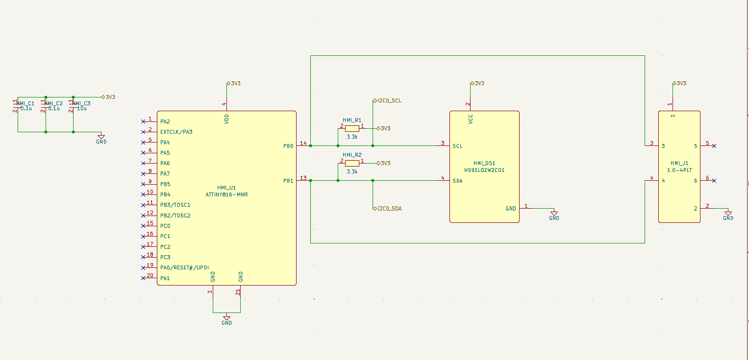
A second example comes from the temperature and humidity sensor KiCad project. Its CHT20MEMS sensor connects to a 3.3 V I2C bus shared with the controller/display subsystem. The generated sheet makes the rail and bus names visible, but the engineer still has to confirm where the effective pull-ups live, whether the display module adds another pair, and whether the chosen values work at the intended clock rate.

KiCad I2C Pull-Up Review Checklist
| Review area | What to check | Why it matters |
|---|---|---|
| Bus voltage | Pull SDA and SCL to a voltage compatible with every connected pin. | A pull-up to the wrong rail can violate input limits or back-power an unpowered domain. |
| Clock mode | Document 100 kHz, 400 kHz, 1 MHz, or the actual operating range. | The allowed rise time changes with the selected mode. |
| Bus capacitance | Estimate IC pins, traces, branches, connectors, cables, shifters, and probes. | Capacitance sets the maximum usable pull-up resistance. |
| Sink capability | Check VOL and IOL for every bus device. | The weakest output determines the minimum safe resistance. |
| Parallel resistors | Audit pull-ups on modules and calculate their effective parallel value. | Several harmless-looking module pull-ups can create excessive sink current. |
| Power states | Review reset, sleep, switched rails, and partially powered devices. | The bus can leak current or back-power devices when rails turn off in different states. |
| Configuration options | Consider DNP options or alternate footprints when bus loading is uncertain. | Bring-up can tune the value without cutting traces. |
| Measurement access | Add accessible SDA, SCL, ground, and bus-voltage test points. | The final value should be validated on the real board with the intended devices connected. |
| Review record | Write the selected speed, estimated capacitance, calculation, and assumptions in design notes. | A documented choice is easier to revisit when the bus or enclosure changes. |
How to Validate the Value on Hardware
- Populate the intended production device set, including displays, sensor modules, cables, and level shifters.
- Measure both SDA and SCL at the worst expected bus speed and supply voltage.
- Measure rise time between 30% and 70% of the bus voltage. Account for oscilloscope-probe capacitance.
- Confirm the LOW voltage at the device with the weakest sink capability.
- Repeat across power states, temperature range, cable options, and maximum device population.
- Check for ringing, noise, slow plateaus from level shifters, clock stretching, and unexpected pull-ups.
- Update the schematic and BOM with the validated value and the assumptions behind it.
The calculation narrows the design space; the assembled board confirms it. This is part of the broader AI-generated KiCad schematic review process before layout or release.
Common Mistakes
- Using 4.7 kΩ automatically without calculating bus capacitance and rise time.
- Using MCU internal pull-ups as the only pull-ups without checking their value, tolerance, and timing.
- Forgetting that every breakout board may add another resistor pair.
- Pulling the bus to 5 V when one or more pins are not 5 V tolerant.
- Assuming controller support for 1 MHz means every target and level shifter supports Fast-mode Plus.
- Ignoring cables, connectors, long branches, and probe capacitance.
- Checking SDA but not SCL, or testing only at room temperature with one device fitted.
- Treating a schematic calculation as proof that the routed, assembled bus will pass.
How SpeedUp Fits
SpeedUp can turn a product requirement into a structured KiCad schematic draft with named I2C nets, sensor and display sheets, candidate pull-ups, power domains, test points, and design notes. That makes the interface visible enough for an engineer to apply the calculation and review the whole bus instead of copying a disconnected breakout-board circuit.
The generated result is a first engineering draft, not a production-ready reference design. Engineers still verify each device data sheet, calculate and measure pull-ups, validate voltage domains and power states, review footprints and PCB layout, write firmware, test signal integrity, and complete sourcing, safety, compliance, and manufacturing work.
Related SpeedUp Projects and Guides
- BME280 KiCad schematic and I2C sensor checklist — interface mode, address, pull-ups, sensor placement, and footprint review.
- AI-generated KiCad schematic checklist before PCB layout — downstream checks after the interface and resistor values have been reviewed.
FAQ
Do I need pull-up resistors for I2C?
Yes, a normal I2C bus needs SDA and SCL pulled HIGH because connected devices normally use open-drain or open-collector outputs. Some modules already contain pull-ups, so verify the complete bus before adding another pair.
What size pull-up resistor should I use for I2C?
Calculate the allowed range from supply voltage, LOW-level sink capability, bus capacitance, and maximum rise time. Values from about 1 kΩ to 10 kΩ are common in compact systems, but no single value is correct for every bus.
Is 4.7 kΩ always correct for I2C?
No. It is a common starting value for short, moderate-speed buses, but it can be too large for a high-capacitance 400 kHz bus or unnecessarily small for a low-power, low-speed bus. Calculate and measure instead of relying on the convention.
Can I use the microcontroller’s internal pull-ups?
Internal pull-ups are often relatively weak and have broad tolerance. They may be useful for a controlled low-speed case, but they should not be assumed to meet I2C rise-time requirements without checking the MCU data sheet and measuring the complete bus.
Where should I place I2C pull-up resistors?
A short PCB bus normally needs one effective pull-up pair, often placed near the controller or a central bus point for clarity and tuning access. Electrical performance depends on the full interconnect, branches, capacitance, and device population; placement alone does not repair an overlong or overloaded bus.
How do multiple I2C pull-ups combine?
They combine in parallel. Two 4.7 kΩ resistors produce an effective resistance of 2.35 kΩ, while four 10 kΩ resistors produce 2.5 kΩ. Include all fitted modules and development boards in the calculation.
Start Your I2C Hardware Project
Put the calculated pull-ups inside a complete, reviewable product schematic.
Use SpeedUp to turn the product requirements into structured schematic sheets and an editable KiCad first draft for engineering review. Create a free account to begin.
Comments
No comments yet.
Leave a Reply