
Quick Answer
A reliable MAX30102 sensor circuit needs more than the four wires shown on a breakout-board tutorial. For the bare optical module, first provide the 1.7 V to 2.0 V VDD rail and a separate 3.1 V to 5.0 V VLED+ rail. Then verify local bypass capacitors, the VDD-before-VLED power-up sequence, I2C pull-ups, the active-low open-drain interrupt, LED-current return paths, the exact 14-pin footprint, and the optical opening against the skin.
The electrical schematic is only one part of the design. Heart-rate or SpO2 performance also depends on mechanical contact, ambient-light control, temperature, motion, firmware settings, signal processing, and validation on the final product. Use the checklist below to review a KiCad schematic before PCB layout, then verify every limit against the current official MAX30102 data sheet.
Why MAX30102 Circuits Fail After a Breakout-Board Prototype
A development module hides design decisions. It may contain a 1.8 V regulator, I2C level shifting, pull-up resistors, bypass capacitors, and a PCB opening already shaped for the optical package. Connecting that module to a 3.3 V microcontroller does not prove that a bare MAX30102 can use the same single rail or the same bus connection.
The bare part combines sensitive photodetection electronics with pulsed red and infrared LED drivers. The analog supply wants a quiet local loop while the LED supply produces dynamic current. The optical package also has to face the tissue through a controlled opening. A schematic can therefore pass ERC and still fail because the LED current contaminates the analog return, VLED rises before VDD, the interrupt floats, the footprint is mirrored, or the enclosure admits uncontrolled ambient light.
Treat the component as an electrical, optical, thermal, mechanical, firmware, and validation subsystem. That framing is the main difference between copying a hobby module and designing a reviewable wearable board.
MAX30102 Schematic Review Checklist
| Review area | What the schematic should show | Why it matters |
|---|---|---|
| Exact part | MAX30102 orderable part, 14-pin OESIP package, approved symbol and land pattern | Module, package, orientation, and no-connect assumptions are not interchangeable |
| VDD | A regulated 1.7 V to 2.0 V analog rail, normally designed around 1.8 V | The bare sensor is not a single-supply 3.3 V breakout module |
| VLED+ | Both VLED+ pins tied to a 3.1 V to 5.0 V LED rail with local bypassing to PGND | LED pulses need headroom and create a separate dynamic current loop |
| Power sequence | A defined way for VDD to become valid before VLED, including startup and brownout behavior | Incorrect sequencing can couple LED-rail current into the analog power-up path |
| I2C | SCL and SDA nets, one intentional pull-up set, compatible voltage domain, and bus-capacitance budget | Missing, duplicated, or over-strong pull-ups cause communication and power problems |
| Interrupt | INT connected to an MCU input with an external pull-up to a verified logic rail | INT is active-low and open-drain; it must not be treated as a push-pull output |
| Grounding | GND and PGND labels, return-current intent, and one controlled connection strategy | LED current should not flow through the sensitive analog supply loop |
| No-connect pins | Pins 1, 5, 6, 7, 8, and 14 represented as mechanical pads without electrical nets | The data sheet calls for PCB pads for mechanical stability even though the pins are electrically N.C. |
| PCB and optics | Orientation marker, optical window, keepouts, enclosure stack, skin interface, and thermal plan | A correct netlist cannot compensate for a blocked or light-leaking optical path |
| Bring-up | Test access for both rails, I2C, INT, ground, and current measurement where practical | Power, bus, FIFO, saturation, and optical faults need to be separated during debug |
Building a wearable or optical sensor product?
Describe the MAX30102, MCU, dual power rails, optical location, enclosure, communications, and battery-life target. Create a free account to start a reviewable, editable KiCad first draft.
MAX30102 Pinout and the Two Power Rails
The 14-pin module has only a few electrical connections, but each one has a distinct role. SCL is pin 2, SDA is pin 3, PGND is pin 4, VLED+ appears on pins 9 and 10, VDD is pin 11, analog GND is pin 12, and INT is pin 13. The remaining pins are no-connects that still require the defined PCB pads for mechanical stability.
VDD powers the sensor electronics and is specified from 1.7 V to 2.0 V. VLED+ supplies the internal LED drivers and is specified from 3.1 V to 5.0 V. A common implementation uses 1.8 V for VDD and 3.3 V for VLED+, but those values do not remove the need to check regulator tolerance, startup, ripple, source impedance, battery range, and LED-current settings.
Do not connect the bare device to one 3.3 V rail simply because a breakout board accepts 3.3 V at its header. Inspect the breakout schematic first: the board may be translating the host supply into the two required internal domains.
I2C Pull-Ups, Address, and Interrupt
MAX30102 communicates through an I2C-compatible interface at up to 400 kHz. The data sheet lists the 8-bit write and read addresses as 0xAE and 0xAF, which corresponds to the commonly used 7-bit address 0x57. Because the address is fixed, confirm that no other device on the bus uses 0x57 or plan an I2C multiplexer or a separate controller bus.
SDA is open-drain, and the bus needs deliberate pull-ups. Do not add a new pair on every sensor sheet without checking the whole design. Choose the pull-up rail only after verifying the MAX30102 input limits, the MCU input thresholds, every other bus device, any level shifter, the total bus capacitance, and off-state back-power paths. The I2C pull-up resistor calculation guide shows how to turn rise-time and sink-current limits into a usable resistor range.
INT is a separate active-low open-drain output. Give it a pull-up to a logic rail that remains valid in the intended power state. Route it to an interrupt-capable MCU input when the firmware will use FIFO-almost-full, new-data-ready, ambient-light-overflow, or temperature-ready events. Then document how the firmware clears the selected interrupt source; reading status or the associated data register can release the line.
Decoupling, Grounding, and Power Sequencing
Place the VDD bypass network close to pin 11 with a short return to analog GND. Place the VLED+ bypass network close to pins 9 and 10 with a short return to PGND. Capacitor value, voltage rating, dielectric, package, bias derating, and placement all matter; a nominal value in the BOM is not enough. Use the decoupling capacitor value and placement guide to review the physical implementation.
Analog Devices specifically recommends supplying VDD before VLED and notes one implementation technique: make the VLED bypass capacitance about twice the VDD bypass capacitance so the LED rail rises later. The same official note warns that LED current must not flow through any part of the analog supply loop. Separate regulator routing or controlled supply paths may be required; drawing two ground symbols without understanding the PCB return current does not create isolation.
Review every state, not only a clean bench startup. What happens when a battery is inserted slowly, USB appears while the battery is low, a load switch disables only one rail, the MCU enters deep sleep, or VDD browns out while VLED remains present? Capture the allowed rail sequence in the power-tree notes and verify it on the assembled board with an oscilloscope.
PCB Placement, Optical Window, and Thermal Design
The sensor measures reflected red and infrared light. Its position relative to the skin, enclosure window, gasket, adhesive, PCB opening, and nearby light sources can matter more than a perfect-looking schematic. Keep the optical surface unobstructed, control stray light between the LEDs and photodetector, and prevent the enclosure from lifting the sensor away from the intended contact area.
Orientation must be unambiguous from symbol through assembly drawing. Verify the current Analog Devices package outline and land pattern rather than trusting a generic community footprint. Include the N.C. pads for mechanical support, check solder-mask and paste openings, and review the reflow process for the optical package. Protect the cover glass during assembly and cleaning.
Temperature changes LED wavelength and affects measurement interpretation. The official power and temperature note recommends thermal mass around pins 8 to 10 to reduce self-heating effects. That recommendation must be reconciled with the optical opening, small wearable geometry, battery placement, charging heat, MCU heat, and skin-facing materials. Validate the final stack mechanically and thermally rather than treating the breakout-board geometry as universal.
Example From a Real SpeedUp Smart-Ring Project
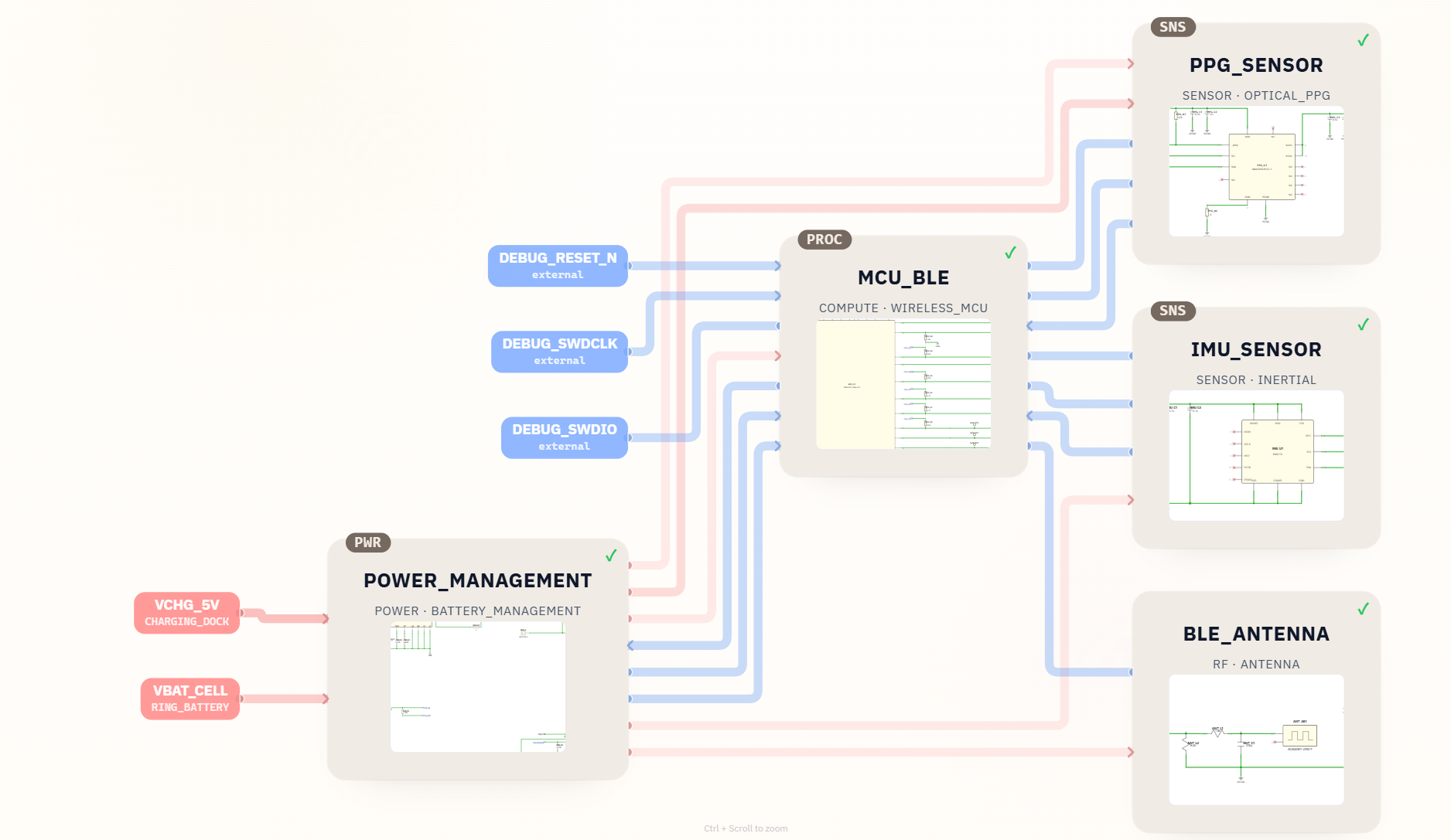
The existing SpeedUp smart-ring circuit project includes a dedicated MAX30102EFD+T sheet. It makes the 1.8 V VDD rail and VLED_PPG rail explicit, gives INT a 47 kΩ pull-up, places local capacitors on both supplies, and separates the PGND and analog-ground labels before a controlled connection. That structure exposes the decisions an engineer needs to review.

One sheet cannot prove the full design. The reviewer still has to locate the I2C pull-ups elsewhere in the project, confirm logic compatibility, calculate the actual rail sequence, check regulator noise and current, audit the symbol and footprint, and validate PCB return paths. The ring enclosure, skin contact, ambient-light barrier, algorithm, motion compensation, temperature behavior, and measurement performance remain outside this screenshot.
What to Put in a MAX30102 Design Prompt
A useful schematic prompt should describe the product constraints, not just say “add a MAX30102.” Include:
- The exact MAX30102 orderable part and whether the design uses the bare optical module or a purchased breakout.
- Battery, USB, charger, regulator, load-switch, and sleep-state requirements.
- A 1.8 V VDD rail and the chosen VLED+ rail, including startup and shutdown behavior.
- The MCU model, its I/O voltage, the I2C bus speed, every device already on the bus, and who supplies the pull-ups.
- Whether INT is required, which MCU pin receives it, and which wake or FIFO events firmware will use.
- The mechanical contact location, optical-window stack, PCB thickness, enclosure material, and available sensor area.
- Required test points, rail-current measurement options, programming connector, and first-board debug access.
- A requirement to mark every unverified value, symbol, footprint, and optical assumption for engineering review.
For a battery product, also work through the battery-powered sensor circuit checklist. Average sensor current alone does not size the regulator or predict runtime; LED pulse settings, radio bursts, charger states, leakage, brownout behavior, and battery impedance all contribute.
Common MAX30102 Circuit Mistakes
- Copying a breakout-board header connection and applying 3.3 V directly to the bare sensor VDD pin.
- Connecting only one VLED+ pin or omitting a local VLED-to-PGND bypass path.
- Allowing VLED to rise first without checking power-up, shutdown, or brownout sequencing.
- Routing pulsed LED current through the analog ground or regulator return loop.
- Adding I2C pull-ups without checking the pull-ups already present on the MCU board or another sensor.
- Assuming 3.3 V logic compatibility from a module tutorial without verifying the bare-part and MCU limits.
- Leaving the open-drain INT pin without a pull-up or connecting it to a non-wake-capable pin when wake is required.
- Using a mirrored, outdated, or unverified optical-package footprint.
- Treating electrically N.C. pins as absent instead of providing their required mechanical pads.
- Placing the sensor behind an uncontrolled window with light leakage, poor contact, or nearby heat sources.
- Claiming heart-rate or SpO2 accuracy before final mechanical, firmware, algorithmic, population, and regulatory validation.
Bring-Up and Testing Order
- With the sensor disabled where possible, check resistance to ground and inspect the package orientation and solder joints.
- Power the board from a current-limited source. Measure VDD, VLED+, startup order, ripple, and sleep-state current.
- Confirm the I2C idle levels and scan for the 7-bit address 0x57 at a conservative bus rate.
- Read the part ID and revision, issue a software reset, and verify the power-ready behavior.
- Configure a low LED current and conservative sample settings before increasing optical power.
- Observe INT, FIFO reads, overflow flags, and ambient-light behavior while monitoring both supply rails.
- Repeat tests with the final optical window, contact pressure, motion, charging state, radio activity, temperature, and realistic battery conditions.
Analog Devices publishes MAXREFDES1043 as a system-level reference that demonstrates configuration, standby behavior, optical measurement flow, and supporting electronics. Use it to understand the complete subsystem, then verify that every part and assumption still fits your product and the latest documentation.
How SpeedUp Fits
SpeedUp can turn a wearable or optical-sensing requirement into a structured KiCad schematic draft with separate power, sensor, MCU, charging, communication, connector, and test blocks. That gives an engineer a concrete design to inspect instead of starting with an empty canvas or silently copying a breakout board.
The generated project remains an engineering draft. The engineer must verify the exact part, symbol, footprint, rails, pull-ups, sequencing, return paths, PCB layout, optics, firmware, thermal behavior, test results, sourcing, EMC, safety, and any medical or regulatory obligations. Use the AI-generated KiCad schematic review guide as the wider sign-off process.
FAQ
How do I connect a MAX30102 to a microcontroller?
For the bare part, provide regulated VDD and VLED+ rails, connect their grounds with a controlled return strategy, add local bypass capacitors, connect SCL and SDA with one verified pull-up network, and connect the open-drain INT pin with its own pull-up if used. Verify logic levels and power sequencing for the exact MCU and power tree.
Can the MAX30102 run from 3.3 V?
The LED supply can operate at 3.3 V when the full design stays within the current data-sheet limits. The sensor’s VDD rail is separate and specified around 1.8 V, not 3.3 V. A breakout board marked “3.3 V” may contain a regulator or level shifting that the bare device does not include.
What is the MAX30102 I2C address?
The commonly used 7-bit I2C address is 0x57. The data sheet expresses the write and read forms as 0xAE and 0xAF. Check the address format expected by the MCU driver so the read/write bit is not shifted twice.
What is the difference between MAX30100 and MAX30102?
They are related red/infrared optical sensor products, but they should not be treated as drop-in replacements. Pinout, package, supply, register, performance, and firmware assumptions must be checked against the current data sheet for the exact orderable part. Start a new symbol and design review when changing devices.
Does MAX30102 work on the wrist?
MAX30102 is intended for wearable optical sensing, but usable wrist performance is not guaranteed by the component alone. Contact pressure, skin interface, ambient-light blocking, motion, temperature, LED current, sampling, signal processing, enclosure geometry, and validation all affect the result.
How do I troubleshoot a MAX30102 that is not detected?
Measure VDD and VLED+, verify VDD rises first, inspect SCL and SDA idle levels, confirm the pull-ups and logic domain, scan for 0x57 at a lower bus speed, check the footprint orientation and soldering, and make sure another device does not use the same address. A logic analyzer can separate an address or acknowledgement fault from a sensor-configuration problem.
Is a MAX30102 circuit automatically medical-grade?
No. A correct component connection does not establish clinical accuracy, safety, or regulatory compliance. Those claims require a defined intended use, complete hardware and software validation, risk management, manufacturing controls, and the applicable regulatory process.
Start Your Optical Sensor Project
Turn your wearable sensor requirements into a structured, editable KiCad first draft.
Use SpeedUp to turn the product requirements into structured schematic sheets and an editable KiCad first draft for engineering review. Create a free account to begin.
Comments
No comments yet.
Leave a Reply