
Quick Answer
An nRF52840 pinout is only useful after the exact package and orderable part have been selected. Nordic documents different physical assignments for the QIAA aQFN73, QFAA QFN48, and CKAA WLCSP packages, so a symbol or footprint from another variant must not be copied into the schematic. Start by locking the package, then map the power and decoupling pins, RF and crystal connections, SWD access, USB pins, and any NFC functions before allocating flexible GPIO to QSPI, PDM, I2C, SPI, UART, buttons, or LEDs.
For the schematic, use Nordic’s package- and supply-specific nRF52840 reference circuitry as the electrical and layout baseline. A correct-looking symbol is not enough: the selected power configuration changes the required regulator, decoupling, USB, and DC/DC connections, while RF performance depends on following the matching network and reference layout closely. The checklist below organizes those decisions and then applies them to a real SpeedUp-generated nRF52840 KiCad project.
Why the nRF52840 Pinout Must Start With the Package
The nRF52840 is not one universal pin map. Nordic’s current ordering information lists three package families: QIAA in a 7 × 7 mm aQFN package, QFAA in a 6 × 6 mm QFN package, and CKAA in a compact WLCSP package. Their ball or pin counts, physical arrangement, available GPIO, and reference circuitry differ. The suffix also matters when checking the exact orderable device and hardware revision.
That makes package selection an architecture decision, not a late footprint task. A large aQFN package may provide more accessible I/O and a more forgiving assembly path. QFN48 reduces board area but exposes a different set of pins and ties some supply behavior to the package. WLCSP is much smaller but increases escape-routing, fabrication, inspection, and assembly constraints. Use Nordic’s current nRF52840 ordering information to confirm the active order code, package, function variant, and purchasing status before building the KiCad symbol-footprint pair.
| Package decision | What to confirm | Schematic consequence |
|---|---|---|
| QIAA aQFN73 | Exact QIAA function and hardware revision, 73-ball footprint, exposed-pad and assembly requirements | Use the matching QIAA pin table and one approved QIAA reference-circuit configuration |
| QFAA QFN48 | Reduced GPIO set, 48-pin footprint, package-specific supply behavior | Rebuild the symbol from the QFAA assignment table; do not delete pins from a QIAA symbol |
| CKAA WLCSP | 94-ball map, fine pitch, escape strategy, PCB and assembly capability | Use the CKAA reference circuit, land pattern, stack-up assumptions, and production constraints together |
| Orderable suffix | Current order code, function variant, reel or tray option, lifecycle status | Keep the BOM, symbol properties, footprint, and sourcing record aligned to the same part |
nRF52840 Pin Groups to Map Before GPIO Allocation
The nRF52840 has flexible peripheral routing, but flexibility does not make every pin interchangeable. Power, decoupling, RF, crystal, USB, and debug functions need to be placed first. Some GPIO have analog capability, low-frequency recommendations, NFC functions, trace functions, reset behavior, or recommended QSPI use. Treat Nordic’s package-specific pin-assignment table as the source of truth and record every deliberate reuse in the schematic notes.
| Pin group | Examples | What the schematic must show |
|---|---|---|
| Power and ground | VDD, VDDH, VBUS, VSS, VSS_PA | The selected supply mode, rail source, local return path, and every package power pin |
| Regulator and decoupling | DEC1 through DEC6, DECUSB, DCC, DCCH | Only the components required by the chosen reference configuration, with values and connections checked against the current revision |
| RF | ANT, VSS_PA | Reference matching network, antenna or connector strategy, controlled geometry, grounding, and tuning provision |
| Clocks | XC1, XC2, and low-frequency crystal pins where provided | Crystal choice, load network, startup assumptions, tolerance, placement, and firmware clock strategy |
| USB | D+, D-, VBUS, DECUSB | Connector role, VBUS sensing/supply path, protection, return path, and USB-specific decoupling |
| Programming and debug | SWDIO, SWDCLK, optional reset and trace signals | Accessible programming path, voltage reference, ground, reset ownership, and production-test access |
| NFC or GPIO | P0.09/NFC1, P0.10/NFC2 | An explicit decision about NFC use, GPIO reuse, external circuitry, and firmware configuration |
| Flexible peripherals | QSPI, PDM, I2C, SPI, UART, PWM, buttons, LEDs | A pin-allocation table that checks electrical limits, boot/reset states, conflicts, routing, and firmware ownership |
Planning an nRF52840 product?
Describe the exact package, power mode, USB role, RF path, memory, audio, and debug requirements. Create a free account to start a reviewable, editable KiCad first draft.
Choose the Power Configuration Before Copying a Schematic
The nRF52840 power system supports several configurations. A product may supply the normal-voltage domain through VDD, use the high-voltage input through VDDH, provide VBUS for USB detection and the USB signalling regulator, or combine sources under a defined system-power architecture. The allowed arrangement depends on the package and the selected reference configuration. Do not merge fragments from two Nordic examples simply because the capacitor values look similar.
Nordic’s power-supply documentation explains that USB operation requires a valid VBUS supply as well as the main device supply, and that the dedicated USB regulator uses DECUSB decoupling. The main and high-voltage regulators have their own external-component requirements. In the schematic, label the source of each rail, expected voltage range, power-up order, current budget, battery or charger behavior, and what happens when USB is inserted while the product is already powered.
Decoupling values should come from the exact package and circuit configuration, not from a generic microcontroller checklist. Place every required capacitor near its assigned pin in the later PCB layout and keep the quiet and RF-related return paths consistent with the reference layout. The decoupling-capacitor value and placement guide can help document effective capacitance, voltage bias, return paths, and layout intent after the Nordic configuration has been selected.
Review the 32 MHz Clock and Low-Frequency Clock Strategy
The radio depends on a valid high-frequency clock strategy. If the design uses an external 32 MHz crystal, verify the crystal frequency, specified load capacitance, tolerance, equivalent series resistance, drive assumptions, and the capacitor calculation against Nordic’s current guidance and the crystal vendor data. Keep the crystal and its capacitors close to the device and away from noisy switching nodes, high-current edges, and unnecessary vias.
The 32.768 kHz clock is a system choice rather than an automatic requirement. An external low-frequency crystal can support accurate timing and low-power behavior, while an internal source may reduce components with different accuracy and current tradeoffs. Record the firmware clock source, calibration expectations, wireless timing requirements, sleep behavior, and whether the selected package exposes the intended pins. A schematic note prevents firmware from silently assuming a crystal that hardware did not fit.
Treat the RF Circuit and Layout as One Design
The ANT pin does not connect to an arbitrary 50 Ω trace and antenna without context. Nordic’s reference circuitry provides the matching components and its PCB reference files show the geometry and grounding that make those values meaningful. The product’s antenna type, enclosure, battery, display, cable, ground plane, mounting method, nearby metal, and board stack-up can all change the final RF behavior.
Reserve the complete RF zone during schematic capture: reference matching parts, optional tuning positions, antenna or RF connector, controlled-impedance intent, ground stitching, antenna keepout, and a clear boundary from clocks, QSPI, displays, microphones, and power converters. Nordic explicitly recommends following the provided schematic and layout references closely for good RF performance. A generated schematic can expose the intended RF path, but it cannot prove antenna tuning, radiated performance, coexistence, or compliance in the final enclosure.
Add USB, SWD, Reset, and Test Access Deliberately
If the product uses the nRF52840 USB device peripheral, connect the dedicated D+ and D- pins and provide the required VBUS and DECUSB path. Define whether the connector also powers or charges the product, then keep that system function separate from the USB signalling requirement. Review the connector’s CC configuration when USB-C is used, ESD protection, shield strategy, ground return, trace impedance, pair symmetry, VBUS protection, inrush, and the device’s behavior when the cable is attached or removed.
Always retain a practical SWD programming and recovery path. The schematic should expose SWDIO, SWDCLK, ground, and a valid target-voltage reference, with a connector or production-pad pattern that can actually be reached after assembly. Decide whether a reset line is needed and remember that P0.18 can be configured as reset while also appearing in recommended QSPI pin assignments. That is a real resource conflict: reserve the function in the pin table before routing QSPI and document how recovery works if firmware or security settings change.
Allocate QSPI, PDM, and Other Flexible Peripherals as a System
The nRF52840 can route many peripheral signals through configurable GPIO, but a valid pin assignment still needs electrical and physical reasoning. For QSPI flash, Nordic identifies the signals SCK, CSN, and IO0 through IO3; its documentation also calls for appropriate high-drive GPIO configuration. Use the recommended pins and reference examples unless the design has a reviewed reason to deviate. Then check routing length, loading, flash supply, decoupling, reset or hold behavior, sleep current, write-protect strategy, and firmware pin configuration. The QSPI flash circuit-design guide covers the memory-side decisions in more detail.
A PDM microphone normally needs a clock output and data input, plus a clean supply and an acoustic placement strategy. Decide whether the design uses mono or a left/right pair, confirm the microphone’s channel-select behavior, and keep the clock away from the RF area and sensitive analog rails. The schematic should show the microphone supply filtering, PDM_CLK, PDM_DIN, channel selection, grounding, test access, and firmware ownership. Continue with the PDM microphone circuit-design guide for timing, power, placement, and signal-integrity considerations.
Apply the same discipline to I2C, SPI, UART, PWM, ADC, buttons, LEDs, and wake inputs. Check level compatibility, pulls, edge rate, drive strength, input state during reset, current when an external device is unpowered, wake behavior, connector exposure, ESD path, and whether firmware can keep the pin in a safe state through boot, update, sleep, and fault conditions.
nRF52840 Schematic Checklist Before PCB Layout
| Review area | Pass condition before layout | Evidence to retain |
|---|---|---|
| Orderable device | Package, function variant, hardware revision, lifecycle, and sourcing match the BOM | Nordic ordering record and approved MPN |
| Symbol and footprint | Every pin comes from the selected package table and maps to the verified land pattern | Pin audit and footprint drawing revision |
| Power mode | VDD, VDDH, VBUS, regulator, and source-switching behavior follow one supported configuration | Power tree, voltage ranges, operating-state table |
| Decoupling and DC/DC | DEC, DCC/DCCH, inductor, and capacitor connections match the current reference circuit | Configuration number, BOM values, placement notes |
| Clocks | HF and LF clock sources, loads, tolerances, and firmware assumptions are explicit | Crystal calculations and clock-source decision |
| RF | Matching network and PCB geometry follow a Nordic reference, with antenna and tuning plan defined | Reference-layout version, stack-up, keepout, RF test plan |
| USB | D+/D-, VBUS, DECUSB, connector role, protection, and attach/detach behavior are complete | USB power/data diagram and protection selection |
| Programming | SWD, voltage reference, ground, reset/recovery, and production access are reachable | Programming fixture or connector drawing |
| Peripheral allocation | QSPI, PDM, I2C, SPI, UART, ADC, and GPIO assignments have no hidden conflicts | Shared hardware-firmware pin table |
| Low-power states | Every external pin has a safe state during reset, sleep, System OFF, and partial power | State table with pulls, leakage, wake ownership |
| Layout handoff | RF, crystals, decoupling, USB, QSPI, and noisy power paths have explicit constraints | Annotated constraints and reference-file links |
| Validation | Power, current, clocks, RF, USB, interfaces, sleep, and recovery have measurable acceptance criteria | Bring-up and product validation plan |
Example From a Real SpeedUp nRF52840 KiCad Project
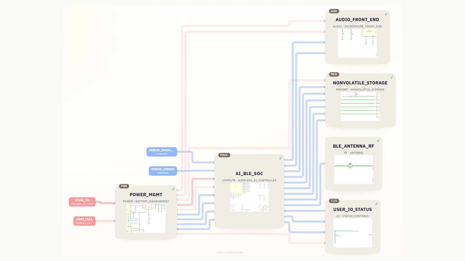
The magnetic AI microphone KiCad project shows how these pinout decisions appear inside a complete product architecture. SpeedUp generated a first schematic draft with separate sheets for power management, the nRF52840 compute block, a PDM microphone, QSPI storage, BLE antenna and RF, and user I/O. The compute sheet uses NRF52840-QIAA-F-R7 and connects clocks, SWD, QSPI, PDM, RF, wake, and LED-status signals.

| Project subsystem | Generated evidence | What still requires engineering review |
|---|---|---|
| nRF52840 compute | NRF52840-QIAA-F-R7, clocks, debug, GPIO, RF feed, storage and audio interfaces | Pin-by-pin package audit, reference-circuit match, orderable revision, power mode, and firmware allocation |
| PDM audio | SPH9855LM4H-C microphone path with clock and data signals | Mic supply noise, timing, channel selection, acoustic port, placement, and continuous-buffer behavior |
| QSPI storage | GD5F1GQ5REYIGR external memory and six-signal QSPI interface | Supported command set, voltage, pin drive, routing, sleep current, endurance, and file-system strategy |
| Power management | Charger, load switch, regulated rail, fuel gauge, and system-power nets | nRF52840 supply configuration, sequencing, peak current, standby current, charging thermal limits, and faults |
| BLE RF | Dedicated antenna/RF sheet and an RF connection from the SoC | Nordic reference-layout match, antenna keepout, enclosure effects, tuning, coexistence, and RF validation |
This is the intended SpeedUp workflow: turn a product brief into an electronics architecture and editable KiCad sheets, then inspect the component-specific decisions while they are still easy to change. The generated package is not an official Nordic reference design and should not be used to replace Nordic’s product specification, reference circuitry, or qualified layouts. Nordic also publishes complete nRF52840 DK hardware files, including schematics and layout resources, that provide an additional authoritative comparison point.
Common nRF52840 Schematic Mistakes
- Using a QIAA symbol with a QFAA or CKAA footprint because the device name looks the same.
- Copying capacitor and inductor values from a different power configuration or an old hardware revision.
- Connecting VBUS for charging while omitting the device’s USB supply and detection requirements, or assuming VBUS alone powers every internal domain.
- Leaving DEC, DCC, DCCH, RF-ground, or exposed-pad connections implicit instead of matching the selected reference circuit.
- Moving the RF matching network or changing its geometry without treating component values and layout as one RF design.
- Allocating
P0.18to QSPI before deciding whether the product needs a hardware reset path. - Using NFC pins as ordinary GPIO without documenting firmware configuration and external-circuit limits.
- Assigning QSPI or PDM pins from logical convenience while ignoring recommended pins, drive settings, routing, and power states.
- Providing SWD pads without target voltage, ground, fixture clearance, or a recovery plan after enclosure assembly.
- Assuming a generated first draft proves RF, USB, low-power current, timing, firmware, sourcing, or production readiness.
How SpeedUp Fits
SpeedUp can turn a plain-language device brief into a system architecture and structured, editable KiCad schematic sheets. For an nRF52840 product, the prompt should state the exact package or module preference, supply and charging path, required wireless protocols, USB role, antenna approach, sensors, audio, storage, connectors, operating states, sleep target, debug access, and mechanical constraints. Those requirements give the generated first draft enough context to expose the power tree, pin allocation, subsystem interfaces, BOM candidates, and review gaps.
The engineer still owns the package-specific pin audit, component calculations, Nordic reference-circuit match, RF layout and tuning, USB implementation, firmware pin configuration, current measurement, sourcing approval, PCB layout, compliance, manufacturing, and hardware validation. SpeedUp helps make the starting point concrete and editable; it does not turn that starting point into a production release automatically. The broader KiCad schematic generator workflow explains how a product prompt becomes reviewable engineering artifacts.
Related nRF52840 Design Resources
- Magnetic AI microphone KiCad project — the complete nRF52840 project example used in this guide.
- QSPI flash circuit design — memory selection, pins, decoupling, routing, and firmware assumptions.
- PDM microphone circuit design — clock, data, power, placement, and audio-path decisions.
FAQ
What is the nRF52840 pinout?
It is the package-specific assignment of power, ground, regulator, RF, clock, USB, debug, NFC, analog, and GPIO functions. There is no single physical pinout shared by the QIAA aQFN73, QFAA QFN48, and CKAA WLCSP packages, so always open the table for the exact orderable variant.
What voltage does the nRF52840 use?
The device supports multiple supply configurations, including normal- and high-voltage paths, while USB uses a dedicated VBUS input and internal signalling regulator. The correct voltage range and external components depend on the package and selected power configuration. Use Nordic’s current power chapter and matching reference circuit instead of relying on one nominal voltage.
Does the nRF52840 support USB?
Yes. It includes a USB 2.0 full-speed device controller with dedicated D+, D-, VBUS, and USB-regulator decoupling requirements. A finished product also needs the correct connector role, protection, power path, routing, firmware behavior, and validation.
Which pins should be used for nRF52840 QSPI flash?
The QSPI peripheral uses SCK, CSN, and IO0 through IO3. Nordic documents recommended pins and reference examples, while the peripheral uses pin-select configuration. Start with the recommended mapping, check conflicts such as reset on P0.18, set the required drive behavior in firmware, and review the complete memory circuit and layout.
Can the nRF52840 connect directly to a PDM microphone?
It includes a PDM interface that provides a clock output and data input for compatible digital microphones. The schematic still needs the correct microphone supply, decoupling, channel selection, GPIO mapping, acoustic placement, and firmware buffering strategy.
Start Your nRF52840 Project
Turn your nRF52840 requirements into an editable KiCad starting point.
Use SpeedUp to turn the product requirements into structured schematic sheets and an editable KiCad first draft for engineering review. Create a free account to begin.
Comments
No comments yet.
Leave a Reply