
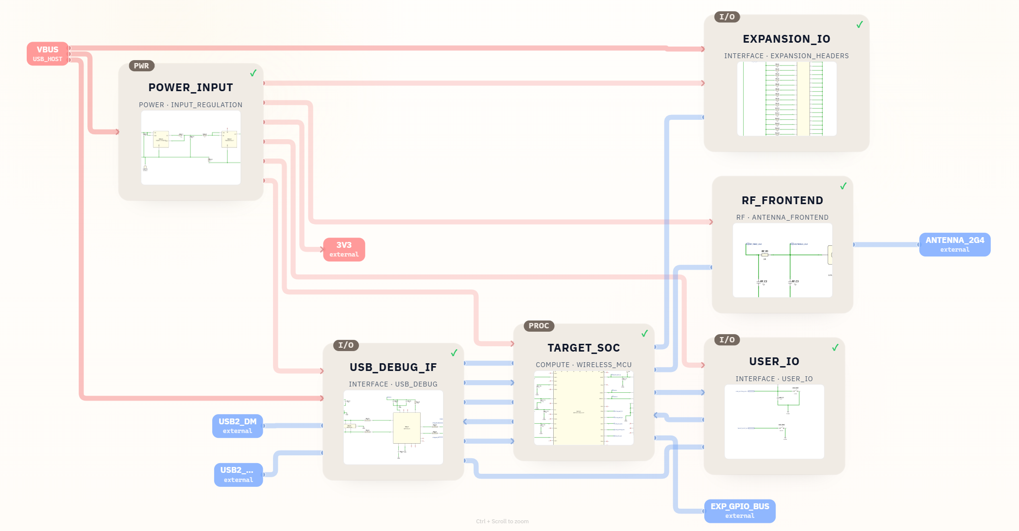
This project shows how SpeedUp turns a one-line hardware idea into a reviewable nRF54L15 DK-style KiCad schematic project. It is a concrete AI schematic generator example: from the prompt, SpeedUp generated a modular development-board draft with power input, USB-C debug, target SoC, RF frontend, expansion IO, user IO, a BOM preview, and a downloadable source package.
If you are looking for the authoritative nRF54L15 pinout, do not copy the provisional target symbol in this generated package. Nordic publishes separate pin assignments for each supported package; use the package-specific datasheet table and reference layout before assigning GPIO, power, clock, debug, or RF pins.
This is a first engineering draft for review, not an official Nordic nRF54L15 DK schematic or production-ready Nordic reference design. The value of the project is that it gives engineers a concrete starting point to inspect, replace, validate, and iterate.
Project Summary
| Field | Details |
|---|---|
| Project | nRF54L15 DK-style development board concept |
| Input | Natural-language prompt |
| Output | DK-style KiCad schematic project generated from a prompt |
| Key modules | POWER_INPUT, USB_DEBUG_IF, TARGET_SOC, RF_FRONTEND, EXPANSION_IO, USER_IO |
| Included files | KiCad project, top-level schematic, six module sheets, BOM CSV/XLSX, symbol libraries, footprint libraries, downloadable ZIP |
| Status | First engineering draft for review |
The Prompt
The project starts with a direct hardware request:
Design an NRF54L15 development board
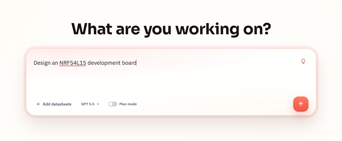
What SpeedUp Generated
SpeedUp turned the prompt into a structured hardware project with:
- A block diagram for the full development board architecture.
- A KiCad project named
nrf54db. - A top-level schematic file,
nrf54db.kicad_sch. - Six module schematic sheets:
POWER_INPUT.kicad_sch,USB_DEBUG_IF.kicad_sch,TARGET_SOC.kicad_sch,RF_FRONTEND.kicad_sch,EXPANSION_IO.kicad_sch, andUSER_IO.kicad_sch. - A BOM preview in CSV and XLSX formats.
- Local symbol and footprint libraries for the generated project.
- A downloadable ZIP package for engineering review.
For searchers comparing nRF54L15 DK schematic examples or AI circuit design tools, this example is intentionally evidence-heavy. Instead of only describing an AI circuit diagram generator workflow, it shows the prompt, generated architecture, KiCad schematic hierarchy, BOM preview, subsystem schematics, and source package that an engineer can inspect.
Want to create an nRF54L15 board?
Describe your own nRF54L15 development board requirements and create a free account to start a reviewable engineering draft.
Project Architecture
The generated design is organized around six main blocks:
POWER_INPUT: takes USB VBUS, adds input protection, generates 3.3 V, and exposes test points for power review.USB_DEBUG_IF: provides USB-C, USB 2.0 data protection, a USB-to-UART bridge, and a manual debug header.TARGET_SOC: contains the Nordic target SoC area, crystals, decoupling, SWD access, GPIO signals, UART links, LED, button, and RF feed.RF_FRONTEND: exposes the 2.4 GHz RF path through a U.FL connector and matching network placeholders.EXPANSION_IO: breaks out selected GPIO and power rails through a 2×20 expansion header.USER_IO: adds a status LED and user/reset buttons for basic development-board interaction.
The important SEO and engineering point is that this is not only a picture of a board idea. The downloadable package includes schematic sheets and BOM data that can be opened, checked, and revised.
nRF54L15 DK-Style KiCad Schematic Output
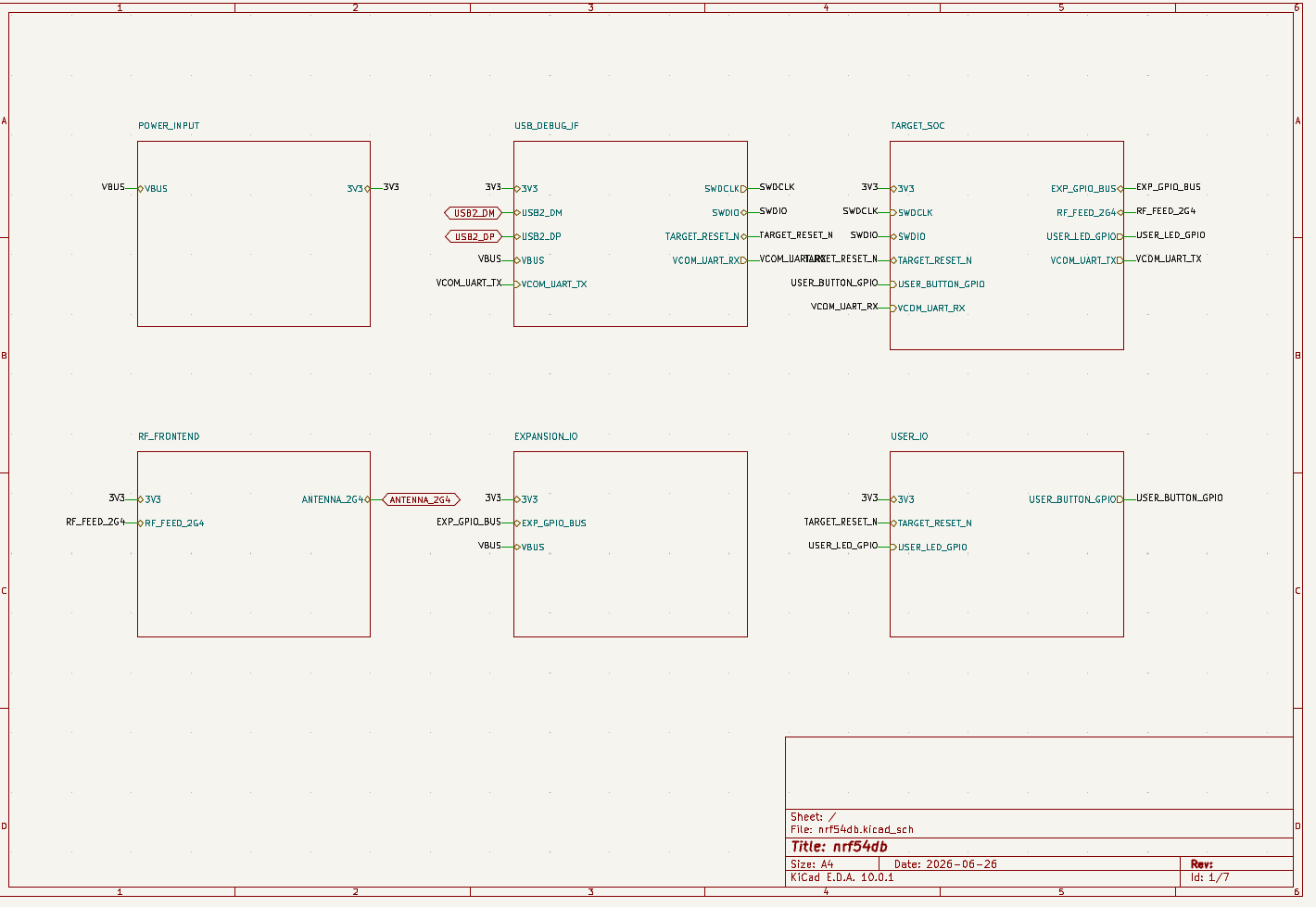
The source package includes nrf54db.kicad_pro, nrf54db.kicad_sch, the six generated module sheets, BillOfMaterials.csv, BillOfMaterials.xlsx, symbol libraries, and footprint files. That makes the DK-style schematic project more useful than a static diagram because the design can move into normal engineering review.
Generated Project vs. the Official nRF54L15 DK Hardware Files
Search results for nRF54L15 schematic and nRF54L15 development board are led by Nordic Semiconductor hardware resources. Those official files and this SpeedUp project serve different purposes: Nordic provides the authoritative DK implementation, while this page documents a generated, editable KiCad starting point and the review gaps it exposes.
| Resource | What it contains | How to use it |
|---|---|---|
| Official Nordic nRF54L15 DK hardware documentation | Official DK schematics, PCB layout resources, BOM, Gerber files, debugger, power, RF, and board-control implementation | Treat as the authoritative reference for the Nordic development kit |
| This generated SpeedUp project | Editable KiCad hierarchy, subsystem sheets, BOM preview, local libraries, screenshots, and a downloadable review package | Use as a prompt-to-KiCad workflow example and an engineering review starting point, not as a clone of the official DK |
Target SoC and RF Review
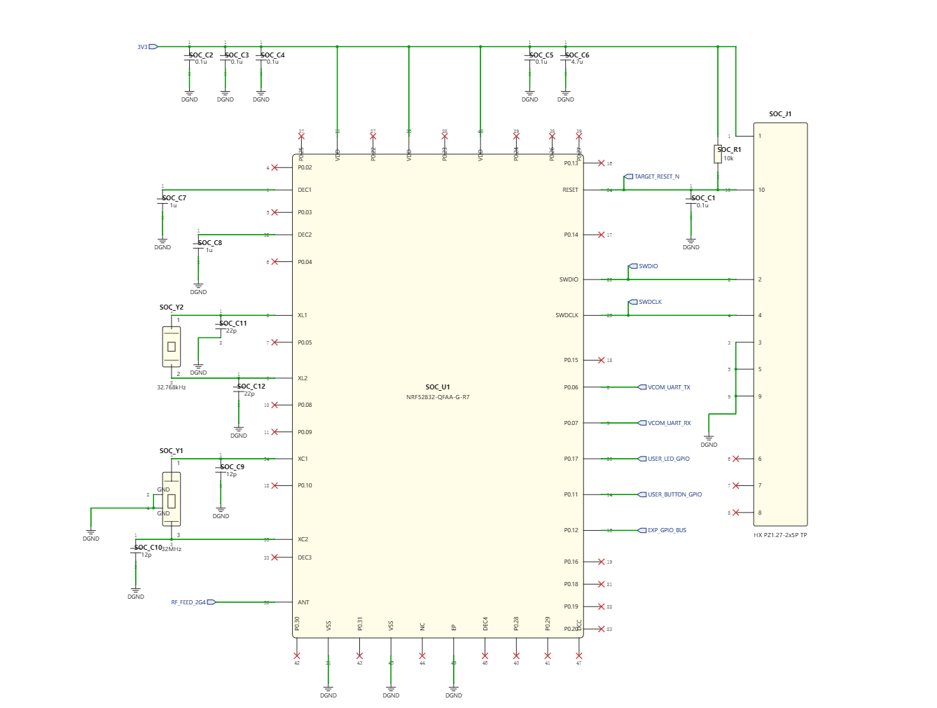
The prompt asks for an nRF54L15 development board, and the generated output is best treated as a DK-style first draft rather than an official nRF54L15-DK reference design. In the generated BOM, the target SoC line uses NRF52832-QFAA-G-R7 as a provisional Nordic QFN-48 surrogate because an exact nRF54L15 component symbol was not available in the source database. That is exactly the kind of issue a first engineering draft should surface early.
Before layout, an engineer should replace or validate the final nRF54L15 symbol, pinout, package, power pins, decoupling plan, crystal requirements, boot/debug pins, GPIO allocation, and RF reference design against Nordic documentation. The generated sheet is a useful scaffold, not a final authority.
nRF54L15 Pinout and Package Selection
There is no single package-independent nRF54L15 pinout to copy into KiCad. Nordic’s current product documentation provides separate pin-assignment figures and tables for four package options. Choose the exact orderable part first, then use the matching table in the official nRF54L15 pin assignments.
| Package | Nordic package code | KiCad review action |
|---|---|---|
| QFN40 | QDAA | Use the QFN40 pin table, mechanical drawing, and matching reference circuit. |
| QFN48 | QFAA | Use the QFN48 pin table and the package-specific QFAA reference layout. |
| QFN52 | QGAA | Use the QFN52 pin table and the package-specific QGAA reference layout. |
| CSP47 | CAAA | Use the CSP47 ball map, mechanical data, assembly rules, and CAAA reference layout. |
The official pin tables distinguish dedicated power, ground, RF, clock, reset/debug, NFC, and GPIO functions. Pin planning also has to respect peripheral and GPIO power domains; a convenient connector label is not proof that a peripheral can use that pin in the intended configuration. Map the non-negotiable pins first, then allocate flexible GPIO and expansion-header signals.
This generated package uses an nRF52832 QFN-48 surrogate, so its symbol and net mapping are not an nRF54L15 pinout. Replace the symbol and footprint together, recheck every unit and hidden power pin, then review local bypass parts with the decoupling capacitor value and placement checklist before layout. Use the KiCad schematic-to-PCB layout checklist for the complete handoff.
nRF54L15 Symbol, Footprint, and Reference Layout Checks
The provisional nRF52832 symbol in this generated package must be replaced before the design can represent an nRF54L15 board. Select the exact nRF54L15 orderable part and package first, then rebuild or import a verified multi-unit symbol, assign the matching footprint, and check every power, ground, RF, crystal, debug, and GPIO pin against the current Nordic product specification.
For PCB work, compare the result with Nordic’s package-specific nRF54L15 reference layout. Nordic recommends following the reference schematic and layout closely for the RF path and matching network. Component values, geometry, placement, stack-up, and trace lengths affect the 50-ohm RF path, so copying only the logical connections is not enough.
- Confirm the exact package variant before choosing the KiCad footprint.
- Validate every symbol unit and hidden power pin against Nordic documentation.
- Copy and review crystal, decoupling, RF matching, grounding, and keepout requirements from the applicable reference design.
- Run KiCad ERC after replacing the provisional symbol, then review unconnected and power-flag warnings manually.
- Do not release PCB layout or RF component values without board-specific review and tuning.
USB-C Debug Interface
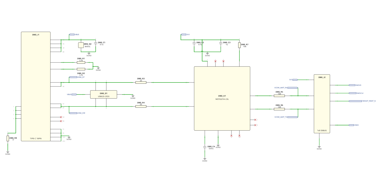
The debug section gives the board a practical bring-up path. It includes a USB-C UFP-style connector, USBLC6-2SC6 low-capacitance USB DP/DM ESD clamp, MCP2221A-I/SL USB full-speed virtual COM UART bridge, 5.1 kOhm CC pull-down resistors, USB series damping resistors, UART isolation resistors, reset pull-up, and a 1×8 debug header.
This subsystem should still be reviewed for USB-C current advertisement, ESD return path, shield bonding, USB trace impedance, bridge power behavior, UART voltage levels, and how SWD, reset, UART, VBUS, and 3.3 V reference are exposed during board bring-up. Apply the USB-C schematic checklist before PCB layout to verify CC resistors, protection, routing constraints, and connector details.
BOM Preview
The generated package includes a BOM preview with 44 line items and 83 placed quantities. Representative entries include:
PWR_U1:SGM6013-3.3YTN5G/TR, a fixed 3.3 V buck regulator.PWR_U2:TPMAX40203AUK+T, a 3.3 V reverse-current blocking switch.PWR_F1:BSMD0805-050-6V, a USB VBUS resettable input fuse.DBG_J1:TYPE-C 16PIN L8.35, the USB-C receptacle.DBG_D1:USBLC6-2SC6, low-capacitance USB DP/DM ESD protection.DBG_U1:MCP2221A-I/SL, the USB-to-UART bridge.SOC_U1:NRF52832-QFAA-G-R7, used as a provisional Nordic QFN-48 surrogate for the requested nRF54L15 target.RF_J1:U.FL-R-SMT(10), a 50 ohm RF connector for the 2.4 GHz path.EXP_J1: a 2×20 2.54 mm expansion header.UIO_D1:SML-310MTT86, a status LED.
The BOM is useful for review, sourcing checks, footprint validation, and cost estimation. It should not be treated as a locked manufacturing BOM until the final SoC, RF path, USB-C behavior, footprints, and component availability have been validated.
What Still Needs Human Review
This project is intended as a first engineering draft. Before treating it as a board-ready design, review:
- Final nRF54L15 symbol, package, pinout, pin mux, power pins, and boot/debug requirements.
- Nordic reference schematics for crystals, decoupling, RF feed, antenna matching, and required keepouts.
- USB-C sink behavior, CC resistors, ESD placement, shield strategy, VBUS protection, and trace impedance.
- 3.3 V regulator current budget, fuse rating, reverse-current path, test points, and power sequencing.
- RF connector placement, 50 ohm controlled-impedance routing, matching network values, ground stitching, and antenna cable keepout.
- Expansion GPIO voltage, current limits, wake-capable pins, ADC-capable pins, and user-accessible power labels.
- Every footprint, land pattern, part availability, and lifecycle status before PCB layout.
- Firmware bring-up assumptions for SWD, UART, reset, LED, user button, and boot configuration.
- Compliance, EMC, safety, and manufacturability requirements for the final board.
Related SpeedUp Projects and Guides
- Read the KiCad schematic generator workflow guide to compare this nRF54L15 project with a broader prompt-to-KiCad workflow.
- Use the AI schematic generator for KiCad circuit projects guide for the higher-level product-to-schematic process behind this example.
- Compare it with the desktop robot ESP32 KiCad project generated from a prompt for another MCU-based generated hardware example.
- Before using the files for layout, follow the AI-generated KiCad schematic review checklist.
FAQ
Where can I find the authoritative nRF54L15 pinout?
Use Nordic Semiconductor’s official nRF54L15 product specification and select the pin-assignment table for the exact package: QFN40/QDAA, QFN48/QFAA, QFN52/QGAA, or CSP47/CAAA. Do not use the provisional nRF52832 symbol in this generated project as an nRF54L15 pinout.
Where can I find the official nRF54L15 DK schematic and PCB files?
Use Nordic Semiconductor’s official nRF54L15 DK hardware documentation and hardware-files download. Nordic identifies the DK package as including official schematics, PCB layout files, a bill of materials, and Gerber files. Compare those authoritative resources with this generated KiCad draft before making component, pinout, RF, power, or layout decisions.
Is this the official nRF54L15 DK schematic?
No. This is a generated nRF54L15 DK-style KiCad schematic project for engineering review, not the official Nordic nRF54L15 DK schematic, layout, or reference design. Use it as a structured starting point, then validate the SoC symbol, pinout, RF path, power tree, USB-C behavior, and BOM against Nordic documentation.
Is this nRF54L15 development board production ready?
No. This is a first engineering draft generated for review and iteration. It should be checked against Nordic documentation, final component symbols, footprints, RF layout rules, USB-C requirements, and manufacturing constraints before production.
Does the generated project use the exact nRF54L15 symbol?
Not yet. The BOM marks NRF52832-QFAA-G-R7 as a provisional Nordic QFN-48 surrogate because an exact nRF54L15 component symbol was unavailable in the source database. That should be replaced or validated before layout.
What files are included in the generated project?
The package includes the nrf54db KiCad project, a top-level schematic, six module schematic sheets, BOM CSV/XLSX files, symbol libraries, footprint files, and the screenshot evidence used in this article.
Can this project be opened in KiCad?
Yes, the package includes nrf54db.kicad_pro and schematic files intended for KiCad review. The screenshots in this article come from those generated project artifacts.
What should engineers review before layout?
Start with the SoC substitution, nRF54L15 pinout, power tree, USB-C interface, RF frontend, crystal requirements, debug connector, expansion header, footprints, and BOM availability. The schematic gives a structured review path, but it is not a final reference design.
Can I generate a similar development board from my own prompt?
Yes. SpeedUp is designed to turn a natural-language hardware idea into structured engineering artifacts such as architecture diagrams, KiCad schematics, BOM previews, and downloadable project files that engineers can review and refine.
Is this an AI schematic generator example?
Yes. The page shows a prompt-to-schematic workflow for a real development-board concept, including a block diagram, KiCad schematic sheets, BOM data, and a downloadable review package. It is still an engineering starting point, not an automatic production release.
Download the nRF54L15 Development Board KiCad Project
Use this package as a review starting point for the generated nRF54L15 DK-style KiCad schematic project. The ZIP includes the nrf54db KiCad project, top-level schematic, module sheets, BOM CSV/XLSX, symbol libraries, footprint files, and source screenshots. It does not replace final Nordic symbol validation, PCB layout, Gerbers, RF tuning, firmware, compliance review, or manufacturing release files.
Create Your Own nRF54L15 Board
Turn your own nRF54L15 development board brief into reviewable engineering artifacts.
Use SpeedUp to generate structured schematic sheets and an editable KiCad project for engineering review. Create a free account to begin.
Comments
No comments yet.
Leave a Reply