
Quick Answer
A breadboard is best when you are still testing the basic circuit idea: trying sensor values, checking firmware behavior, swapping modules, and proving that the product concept can work. A PCB board is the right next step when the wiring has stopped changing, the circuit needs to survive movement, the product needs a fixed shape, or the design depends on power, noise, connectors, RF, battery, thermal, or manufacturing constraints.
The practical middle step is not to jump straight from a messy breadboard to PCB layout. First, turn the working prototype into a clean schematic that captures power rails, connectors, interfaces, part choices, and review risks. A KiCad schematic gives engineers a stable source of truth before footprints, placement, routing, and fabrication decisions start.
SpeedUp can help with that transition by generating a first KiCad schematic draft from a product description. The result is still a review starting point, not a production-ready reference design.
Why This Decision Matters
Breadboards are wonderful when the question is, "Can this circuit idea work at all?" They are fast, reusable, forgiving, and easy to change. That is exactly why they are useful for early exploration.
The same strengths become liabilities when the question changes to, "Can this become a reliable product board?" Breadboard wiring is easy to disturb, hard to document, and weak at representing physical constraints. Long jumper wires, shared rails, loose contacts, and module adapters can hide issues that a PCB must handle deliberately.
PCB design solves a different problem. A PCB board fixes component placement, trace routing, grounding, connector orientation, manufacturing layers, assembly constraints, and mechanical fit. That makes it better for reliability and repeatability, but it also makes mistakes harder to undo.
The safest transition is:
1. prove the behavior on a breadboard or module prototype 2. document the intended circuit as a schematic 3. review the schematic, BOM, footprints, and layout risks 4. move into PCB layout only when the design intent is stable
PCB Board vs Breadboard
| Area | Breadboard | PCB board | What to decide before moving |
|---|---|---|---|
| Best use | Fast circuit experiments and firmware bring-up | Fixed, repeatable hardware for enclosure, assembly, and testing | Has the circuit stopped changing every session? |
| Wiring | Jumper wires and internal breadboard contacts | Copper traces, planes, vias, pads, and connectors | Are signal paths, power rails, and connectors known? |
| Reliability | Easy to disturb and difficult to ship | More robust and repeatable when designed correctly | Does the prototype need to survive movement or repeated use? |
| Frequency/noise | Limited by long wires, parasitics, and weak grounding | Can support controlled grounding, routing, and decoupling | Are analog, RF, fast digital, or power paths involved? |
| Components | Friendly to through-hole parts and breakout modules | Supports SMD packages, modules, connectors, and mechanical constraints | Are final part packages and footprints known? |
| Documentation | Often informal or incomplete | Requires schematic, BOM, layout, and manufacturing files | Can another person understand and rebuild it? |
| Cost of change | Low | Higher after fabrication | Are requirements stable enough for a board spin? |
Ready to move beyond the breadboard?
Describe the working prototype, modules, sensors, power source, connectors, interfaces, and product constraints. Create a free account to start a reviewable, editable KiCad first draft.
This is why "PCB board vs breadboard" is not really a question of which is better. It is a question of which stage you are in.
When To Move From Breadboard To KiCad
Move from breadboard to a KiCad schematic when at least four of these are true:
| Signal | What it means | KiCad review action |
|---|---|---|
| The same wiring has worked more than once | The circuit is becoming stable | Capture the exact connections and net names |
| Firmware is no longer blocked by basic wiring | The MCU, sensor, and interface assumptions are known | Add programming, debug, boot, and test access |
| You know the power source | USB, battery, adapter, or regulated rail decisions are clear | Define power input, protection, regulation, and decoupling |
| The product needs an enclosure or fixed connector positions | Physical layout matters | Add connector orientation, mounting, and keepout notes |
| Jumper wires are causing intermittent behavior | The prototype is outgrowing loose wiring | Replace ambiguous wiring with reviewed nets |
| You need SMD parts or exact modules | Breadboard adapters are no longer enough | Select footprints and verify packages |
| Someone else needs to review or build it | The design needs a shared source of truth | Produce schematic, BOM, and review notes |
| You are preparing for fabrication | The board needs manufacturing constraints | Review footprints, test points, DRC, and layout rules |
Do not wait until the breadboard is perfectly polished. The point of a schematic is to make the design reviewable. It is normal for the first KiCad version to expose questions that the breadboard hid.
Example From a Real SpeedUp Project
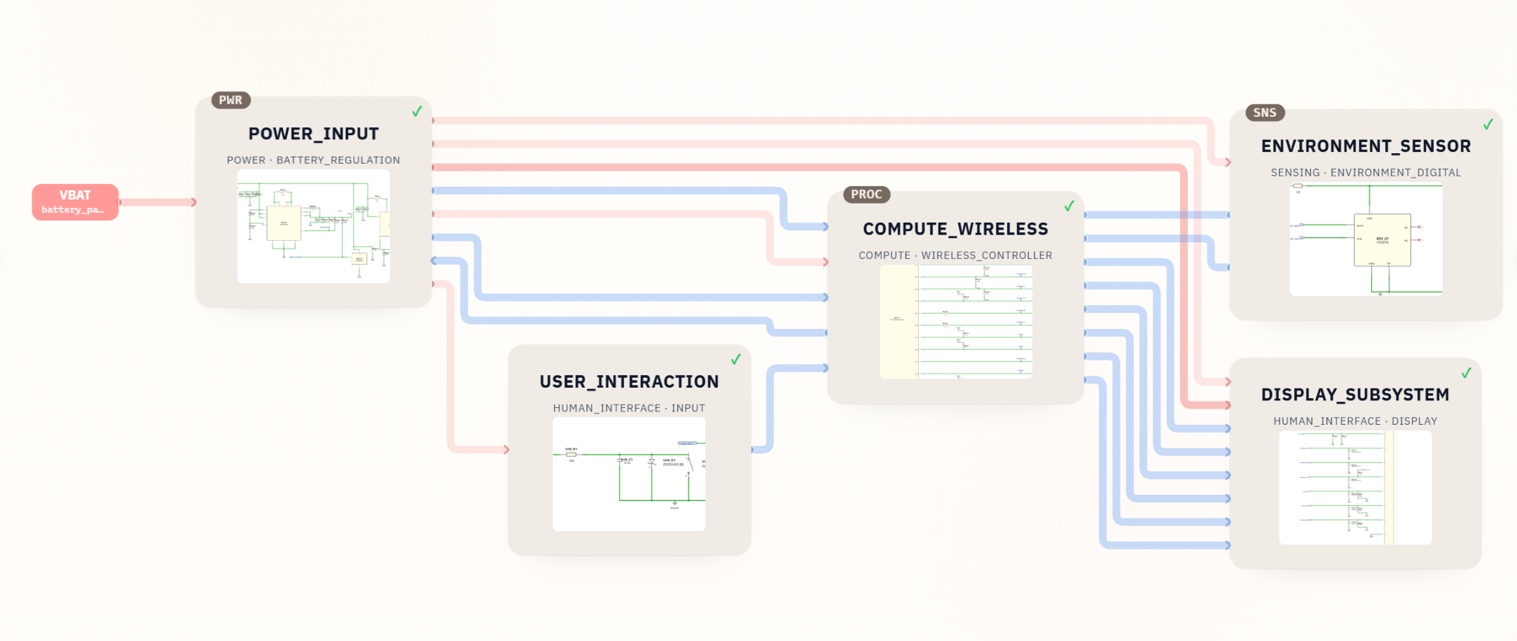
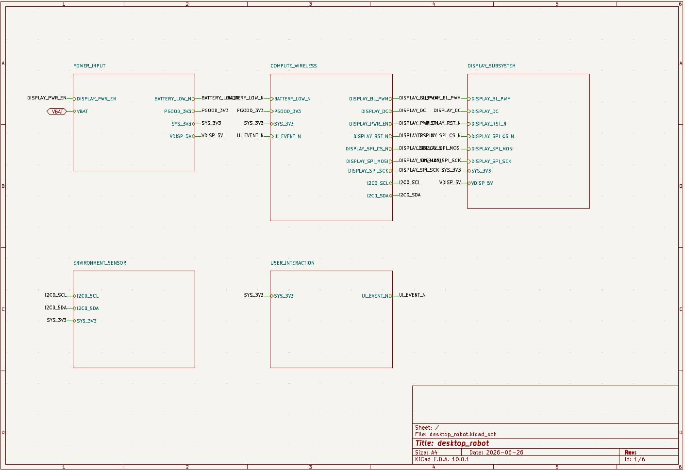
The Desktop Robot ESP32 KiCad project shows what the transition looks like after the prototype idea becomes a structured hardware design. Instead of a pile of modules and jumper wires, the design is organized into reviewable sheets for power, compute, display, sensing, and user interaction.
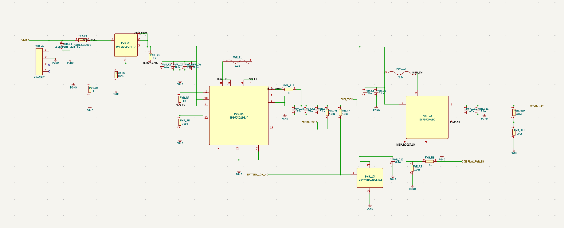
For a breadboard prototype, the power path is often a quick connection to USB, a bench supply, or a regulator module. On a PCB, that becomes a design area that needs protection, current capacity, voltage margin, connector choice, decoupling, and thermal review.
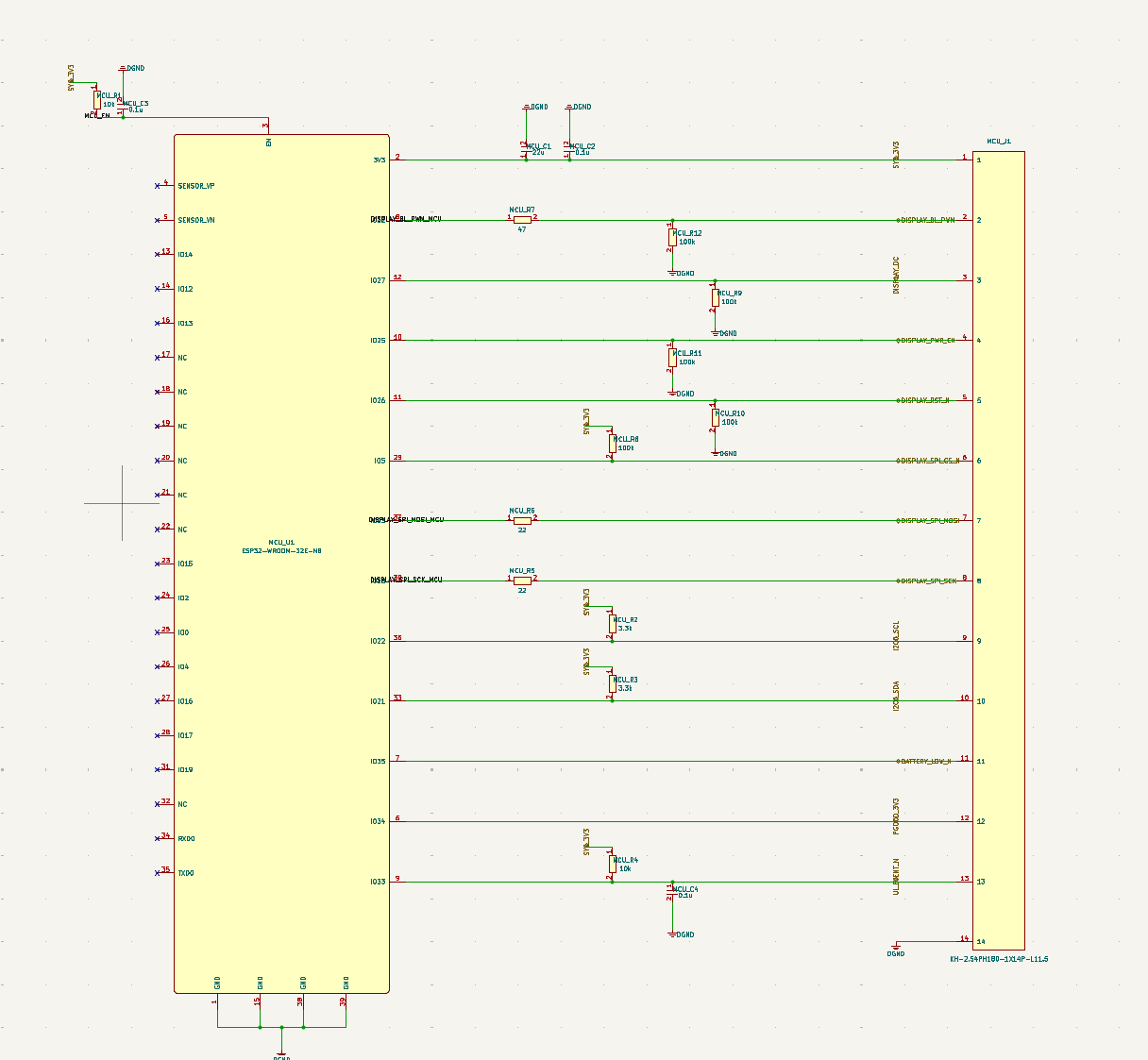
The compute and wireless section is another common transition point. A breadboard might use a development board. A PCB design needs to decide whether the final product keeps a module, uses a bare MCU, exposes programming pins, and protects antenna or mechanical keepout areas.
Breadboard To PCB Review Checklist
Before opening a PCB layout editor, review the schematic with this checklist.
| Review area | What to check | Why it matters |
|---|---|---|
| Power input | USB-C, barrel jack, battery, protection, fusing, switch, reverse polarity | Breadboards often hide power-path assumptions |
| Voltage rails | 5 V, 3.3 V, sensor rails, analog rails, enable pins, load current | PCB reliability depends on real current and thermal margins |
| Grounding | Shared ground, analog/digital split assumptions, return paths, shield or chassis ground | Breadboard ground wires do not represent PCB current loops |
| MCU and firmware | Boot pins, reset, programming/debug header, oscillator, flash, test access | A prototype is painful to debug if the board has no bring-up path |
| Sensors and modules | I2C/SPI/UART pins, pullups, addresses, voltage levels, mechanical placement | Breakout boards often include support parts that the PCB must reproduce |
| Connectors | Pinout, orientation, pitch, locking, strain relief, cable direction | Connector mistakes are common when moving from jumper wires to board edges |
| Footprints | Exact package, pad pitch, pin 1, thermal pad, mounting holes, height | A correct schematic can still fail if the footprint is wrong |
| Test points | Power rails, reset, boot, programming, key buses, sensor signals | Bring-up needs access after the board is assembled |
| Manufacturing | Silkscreen, courtyard, paste, assembly side, DNP options, BOM alternates | The board must be buildable, not only electrically plausible |
This checklist is also a useful prompt for AI-generated schematic review. If the generated project cannot answer a row in the table, mark it as a review item before layout.
Common Mistakes
- Treating the breadboard wiring as the schematic. A breadboard proves behavior, but it does not fully document intent.
- Moving to PCB layout before choosing real part packages.
- Forgetting that breakout modules often include pullups, regulators, level shifting, or protection that must be recreated or intentionally omitted.
- Routing a PCB before adding programming, reset, boot, and test access.
- Assuming a PCB will automatically fix unstable breadboard behavior without understanding the cause.
- Copying a breadboard pin order directly to connector pinout without thinking about cable direction and enclosure access.
- Skipping footprint review because the circuit already worked on a development board.
How SpeedUp Fits
SpeedUp helps turn a product idea into a first KiCad schematic draft. That is useful exactly at the point where a prototype is leaving the breadboard stage and needs a reviewable engineering document.
The best workflow is:
1. describe the device, modules, power source, sensors, and constraints 2. generate a structured KiCad schematic draft 3. review power, interfaces, connectors, footprints, BOM, and test access 4. update the schematic before PCB layout 5. treat the first board spin as an engineering prototype, not production hardware
SpeedUp does not replace engineering review. It gives the team a faster starting point so the review can happen on a real schematic instead of scattered breadboard notes.
Related SpeedUp Projects and Guides
- Desktop Robot ESP32 KiCad Schematic Project Generated from a Prompt – the real project example used in this guide.
- KiCad Schematic Generator: From Product Prompt to Editable KiCad Project – how SpeedUp turns a product description into a KiCad starting point.
- How to Review AI-Generated KiCad Schematics Before PCB Layout – the broader review workflow after a schematic is generated.
- What to Check Before Using an AI-Generated KiCad Schematic for PCB Layout – PCB layout readiness checks.
- Battery Powered Sensor Circuit Design Checklist – a related checklist for power and sensor prototypes.
FAQ
Is a breadboard the same as a PCB board?
No. A breadboard is a reusable prototyping tool for temporary circuit experiments. A PCB board is a manufactured circuit board with fixed copper connections, footprints, holes, layers, and assembly constraints.
Should I always breadboard before making a PCB?
Not always. Breadboards are useful for simple circuits, firmware experiments, and module testing. Some designs, especially RF, high-speed digital, fine-pitch SMD, high-current power, or tight mechanical products, may need schematic review, simulation, breakout testing, or an early PCB prototype instead of a full breadboard build.
When should I move from breadboard to PCB?
Move when the circuit behavior is mostly proven, the wiring is stable, the product needs a fixed shape, or breadboard limitations are getting in the way. Before layout, capture the design as a schematic and review power, connectors, footprints, BOM, and test access.
Can a breadboard prototype become a KiCad schematic?
Yes, but it should be translated thoughtfully. Do not just copy jumper-wire order. Convert the prototype into named nets, modules, power rails, connectors, part choices, and review notes.
Can SpeedUp generate the schematic from my prototype idea?
Yes. Describe the product, modules, sensors, power source, connectors, and constraints, and SpeedUp can generate a first KiCad schematic draft. You should still review and validate the result before PCB layout or fabrication.
Move Your Prototype Into KiCad
Turn the breadboard behavior into a structured schematic that engineers can review and extend.
Use SpeedUp to turn the product requirements into structured schematic sheets and an editable KiCad first draft for engineering review. Create a free account to begin.
Comments
No comments yet.
Leave a Reply