
Quick Answer
A PDM microphone circuit normally needs five electrical connections: a valid supply, ground, a clock from the processor, a one-bit data output back to the processor, and a SELECT connection that determines which clock edge carries the microphone channel. The processor must have a PDM input peripheral or another block that can decimate the high-rate one-bit stream into ordinary PCM audio samples.
The schematic is simple, but the design is not just “connect CLK and DATA.” Confirm that the microphone supply and I/O levels are compatible with the MCU, place local decoupling at the microphone, choose a clock rate supported by both devices, define SELECT instead of leaving it floating, and plan the bottom-port acoustic opening before PCB layout. If two compatible microphones share one data line, configure one for each clock edge and verify that the MCU supports stereo PDM capture.
This guide uses a real SpeedUp project as an example: an SPH9855LM4H-C digital MEMS microphone powered from 1.8 V and connected to the PDM peripheral of an nRF52840. The values shown are evidence from that generated first engineering draft, not universal recommendations. They still need to be checked against the current microphone data, processor configuration, PCB stackup, mechanical design, and prototype measurements.
What Is a PDM Microphone?
A pulse-density-modulation microphone contains the MEMS acoustic sensor, analog front end, converter, and PDM modulator inside the package. Its DATA pin produces a high-rate stream of ones and zeros. The density of those ones represents the instantaneous audio amplitude; the stream is not yet a sequence of conventional 16-bit or 24-bit audio words.
The receiving processor or codec supplies the microphone clock and applies a decimation filter to recover lower-rate PCM samples. That distinction matters when selecting the MCU. A device may have flexible GPIO and an I2S block yet still lack a dedicated PDM input path. Nordic documents that the nRF52840 PDM peripheral generates the microphone clock, performs hardware decimation, supports mono or a two-microphone left/right pair, and moves 16-bit samples to RAM with EasyDMA.
Digital does not mean immune to hardware problems. The audio signal is less exposed to analog interference after conversion inside the package, but poor supply integrity, clock ringing, mismatched logic levels, a blocked acoustic port, or incorrect channel-edge configuration can still produce silence, distortion, channel swaps, or unstable data.
PDM vs I2S vs Analog Microphones
| Microphone output | Typical digital signals | Where conversion or filtering happens | Best fit |
|---|---|---|---|
| PDM | Clock and one-bit data; often SELECT for channel edge | The microphone creates PDM; the MCU, DSP, or codec decimates it to PCM | Compact capture path when the processor has a compatible PDM peripheral |
| I2S | Bit clock, word-select clock, and serial data | The microphone includes decimation and outputs word-oriented digital audio | Processors with I2S but no PDM input, or systems needing a standard serial-audio stream |
| Analog | Analog output plus power and ground | An external ADC or codec converts the signal | Systems with a suitable analog audio path or very specific size, noise, and bandwidth needs |
Analog Devices’ MEMS microphone design comparison explains the key architectural difference: a PDM microphone leaves decimation to the receiving device, while an I2S microphone performs that processing internally and transmits baseband audio words. Choose the interface from the complete signal chain, not from the microphone label alone.
PDM Microphone Pins and Their Jobs
| Pin or net | Direction | What to verify |
|---|---|---|
| VDD | Power into microphone | Operating range, current in each mode, ramp behavior, noise, and local decoupling |
| GND | Return | Low-impedance return path and layout around the acoustic port |
| CLK / CLOCK | MCU or codec to microphone | Allowed frequency, logic level, duty cycle, edge rate, and source termination |
| DATA | Microphone to MCU or codec | Input threshold, active clock edge, shared-line behavior, routing, and idle state |
| SELECT / L-R | Static configuration into microphone | Which level maps the output to which edge; never infer this from another microphone family |
The selected part must be checked by exact orderable number. The current Syntiant automotive microphone portfolio lists the SPH9855LM4H-C as a 1.8 V nominal, bottom-port digital microphone with a 66 dB SNR and 3.50 × 2.65 × 0.98 mm package. Those performance values help with part selection, but the detailed data sheet still controls the schematic, timing, land pattern, and acoustic recommendations.
Designing a digital microphone product?
Describe the processor, PDM microphone, clock and data interface, power, storage, connectivity, and acoustic constraints. Create a free account to start a reviewable, editable KiCad first draft.
Design the PDM Microphone Power Path
Match both the supply range and the digital I/O domain
Start by comparing the microphone VDD range with the rail that will power it. Then compare the microphone clock-input threshold and data-output levels with the MCU’s I/O domain. A microphone that can operate from 1.8 V should not automatically be connected to a 3.3 V clock. Conversely, a 1.8 V data output must still meet the MCU’s input-high threshold under worst-case voltage, process, and temperature conditions.
If the two sides use different domains, select level translation that can handle the required clock frequency and signal direction. CLK is driven toward the microphone; DATA is driven back toward the processor. A bidirectional I2C-style translator is generally not a substitute for analyzing these push-pull digital paths.
Place local decoupling at VDD
The microphone’s internal analog and digital circuitry both depend on its supply. Follow the exact manufacturer’s bypass recommendation and place the high-frequency capacitor close to VDD and GND with a short return. If the source rail is shared with a radio, switching regulator, memory, display, or other burst load, evaluate whether a ferrite bead or small resistor plus a local reservoir is justified.
A series element and capacitors form a filter whose impedance, voltage drop, startup behavior, and transient response depend on real component values and the microphone current profile. Copying a 10 Ω resistor from another schematic without checking those conditions can create a slow or sagging supply. Treat the network as a designed power path, not decorative filtering.
Choose and Route the PDM Clock
The processor normally acts as the PDM clock master. Its selected clock must fall within a mode supported by the microphone and must produce the intended PCM sample rate after decimation. Do not pick a familiar round frequency without checking both documents. The microphone may have separate low-power and normal-performance clock bands, while the MCU may expose only a defined set of generator values and decimation ratios.
For example, the nRF52840 documentation specifies a 16 kHz, 16-bit PDM output path with a selectable clock-to-output ratio of 64 or 80. That is useful system information, but it is not permission to choose either ratio blindly. The resulting actual clock must also sit inside a valid operating band for the exact microphone. Confirm the final register setting, generated frequency, microphone mode, and expected audio bandwidth together.
CLK is a fast digital edge even when the frequency is only a few megahertz. Keep its path short, give it a continuous return plane, and avoid routing it beside the microphone supply, antenna feed, high-impedance analog nodes, or sensitive sensor traces. Analog Devices notes that a small source-series resistor can reduce ringing on longer clock routes, but the need and value depend on the driver, trace impedance, load, and measured waveform. If used, place it near the clock source.
Route PDM DATA and Configure SELECT
DATA returns the one-bit stream to the MCU input. Give it the same basic signal-integrity attention as CLK: short routing, a clean reference plane, compatible logic thresholds, and no unnecessary stubs. Name the nets by role—such as AUDIO_PDM_CLK and AUDIO_PDM_DATA—so that direction and intent remain visible across hierarchical sheets.
SELECT determines which clock edge a microphone uses to drive its data. In a mono design, tie SELECT to the level required for the channel that the MCU will sample. In a two-microphone design, compatible microphones can share CLK and DATA while one is assigned to each edge. The nRF52840 supports this left/right arrangement and can swap edge interpretation in its MODE configuration.
Do not leave SELECT floating, and do not assume that “low means left” is universal. Check the exact microphone data sheet, then document the chosen edge in the schematic and firmware pin table. For a stereo pair, use the same microphone type unless the vendors explicitly guarantee compatible timing; even small timing or sensitivity differences can complicate synchronized capture.
Connect the PDM Microphone to the MCU
Before assigning pins, answer four questions:
- Does the MCU have a real PDM receive path? A timer and GPIO may generate and sample signals in a prototype, but a dedicated peripheral with decimation and DMA is usually the safer system choice.
- Can the PDM signals map to the intended physical pins? Confirm package pin availability, pin multiplexing, reset state, and conflicts with flash, radio, debug, or other peripherals.
- What PCM format will firmware receive? Check sample rate, word width, mono/stereo order, gain, buffer alignment, and DMA requirements.
- What happens during start and stop? Account for microphone wake-up and filter settling. Nordic advises discarding initial samples because startup transients can be present.
The hardware and firmware specifications should use the same names and assumptions. Record the clock frequency, ratio, selected edge, mono/stereo mode, gain, sample format, and buffer strategy. A schematic that says only “PDM to MCU” leaves too many integration decisions hidden.
Example: SPH9855LM4H-C With an nRF52840

This project sheet makes the important connections explicit. The SPH9855LM4H-C is powered from the AVDD_MIC_1V8 rail through R21, a 10 Ω series resistor. C38 provides 1 µF of local capacitance and C39 provides 0.1 µF close to the microphone supply. CLOCK and DATA leave the sheet as AUDIO_PDM_CLK and AUDIO_PDM_DATA. SELECT is tied to ground for a defined mono channel.
Those choices create a review list rather than a claim that the circuit is finished:
- verify the 1.8 V rail and nRF52840 GPIO levels against the exact microphone revision;
- calculate the voltage drop and startup response of the 10 Ω supply element;
- place C38 and C39 so their return path is genuinely local to the microphone;
- select an nRF52840 PDM clock and ratio that fall inside the microphone’s valid clock mode;
- confirm that SELECT tied low matches the firmware’s sampled edge;
- verify the exact footprint, bottom-port opening, paste and mask geometry before layout; and
- measure the clock, supply, startup samples, noise floor, and captured audio on a prototype.

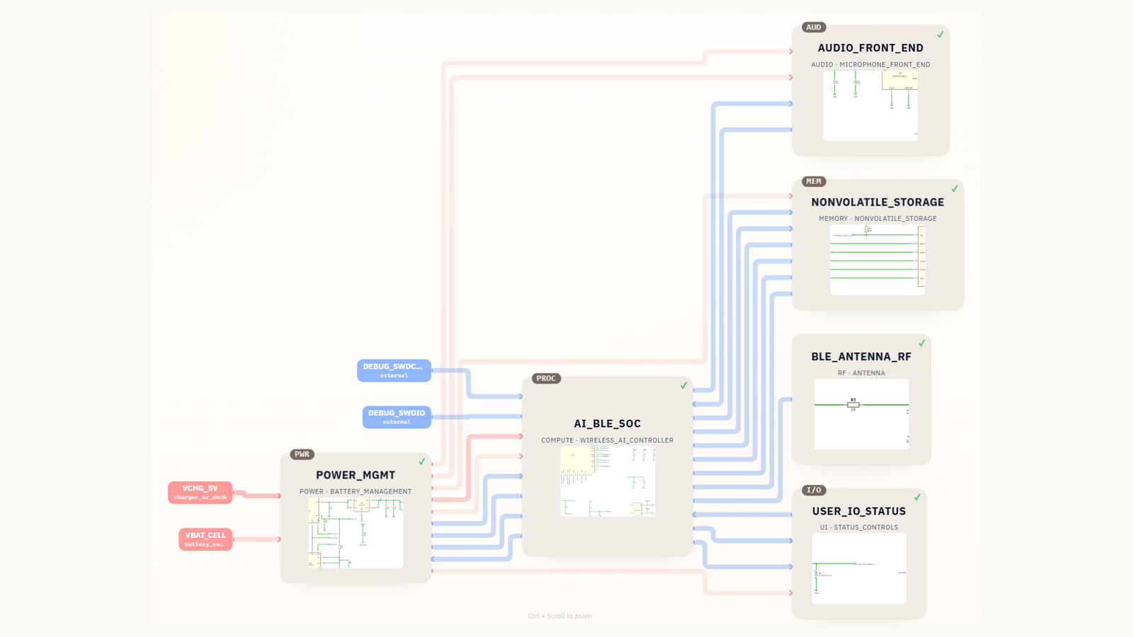
The microphone is one part of a larger battery-powered recorder architecture with BLE, QSPI storage, charging, power regulation, debug, and user controls. See the complete magnetic AI label microphone KiCad project for the original product prompt and the other generated sheets.
Plan the PCB and Acoustic Path Together
A bottom-port MEMS microphone needs a deliberate opening through the PCB. The manufacturer’s land pattern, acoustic-hole diameter, solder-mask clearance, paste pattern, keepout, and cleaning guidance are part of the component interface. Do not replace them with a generic LGA footprint that happens to share the package outline.
The enclosure must deliver sound to that port without creating a leak, cavity resonance, or blocked path. Coordinate the PCB hole with the gasket, enclosure opening, microphone orientation, ingress protection, and manufacturing tolerances. Keep copper, vias, and debris away from the acoustic opening as required by the microphone documentation.
Placement also affects system noise. Separate the microphone from inductors, vibrating motors, relays, speakers, airflow, enclosure creaks, and high-current switching paths. A digital microphone reduces exposure of the audio signal after conversion, but it does not prevent mechanical noise from reaching the sensor or supply noise from modulating the microphone electronics.
Common PDM Microphone Circuit Mistakes
- Choosing the interface after the MCU. The selected processor has I2S but no suitable PDM input or decimation path.
- Checking VDD but not I/O levels. The microphone supply works, but the MCU clock or input thresholds are incompatible.
- Leaving SELECT undefined. The captured channel is silent, intermittent, or interpreted on the wrong edge.
- Assuming every clock setting is valid. The MCU produces a frequency between the microphone’s documented operating modes.
- Copying a clock resistor. A series value is added without considering the source driver, route, loading, or waveform.
- Putting decoupling far from the microphone. The capacitor exists in the schematic but not in the high-frequency current loop.
- Using a generic footprint. The pads look plausible while the bottom acoustic port or paste pattern is wrong.
- Ignoring startup samples. Firmware treats filter or microphone transients as valid audio.
- Calling the first draft production-ready. No clock, noise, acoustic, assembly, or captured-audio measurements have been completed.
PDM Microphone Schematic Checklist
- Exact microphone manufacturer part number and current data sheet recorded
- VDD operating range, current modes, and I/O logic levels confirmed
- Clock source, actual frequency, duty cycle, and decimation ratio documented
- MCU PDM peripheral, physical pin mapping, sample format, and DMA plan confirmed
- SELECT tied to a defined level and matched to the firmware edge setting
- Mono or shared-data stereo topology documented
- Local bypass parts and return path placed at the microphone
- Optional clock source termination reserved or justified by layout analysis
- Bottom-port land pattern and PCB acoustic opening copied from the exact data sheet
- Enclosure acoustic path, gasket, contamination, and mechanical noise reviewed
- Prototype plan includes supply, clock, startup, noise-floor, and audio-capture measurements
Prototype Validation Plan
Bring up the interface in layers. First confirm the microphone VDD at the package, including startup and any droop while capture is active. Next probe CLK at the microphone rather than only at the MCU pin; record its actual frequency, amplitude, duty cycle, overshoot, and ringing. Then inspect DATA and verify that activity appears on the edge selected by the microphone and receiver configuration.
Capture a known acoustic input and check the resulting PCM stream for channel order, sample rate, clipping, dc offset, idle noise, missing buffers, and startup transients. Repeat the test with the radio, storage, charger, display, and other noisy system blocks active. A clean bench capture with those blocks disabled does not describe the finished device.
Finally, evaluate the assembled enclosure. Compare open-board and enclosed frequency response, sensitivity, mechanical handling noise, airflow sensitivity, and consistency across several units. These measurements reveal problems that a schematic cannot: an obstructed port, poor gasket seal, cavity resonance, contamination, or vibration coupled through the PCB. Save the firmware settings and test conditions with the results so that a later hardware revision can be compared against the same baseline.
How SpeedUp Fits
SpeedUp helps turn a product brief into an architecture, structured circuit sheets, component selections, and an editable KiCad first draft. For a PDM microphone product, the brief can state the microphone interface, processor family, audio sample requirements, power source, storage, radio, controls, and enclosure constraints. The generated project then gives the engineering team a concrete artifact to review instead of a blank schematic.
The handoff is deliberately editable and reviewable. Engineers still own the exact part data, timing, supply integrity, footprint, PCB and acoustic layout, firmware configuration, prototype measurements, and production decisions. The embedded-system architecture guide shows how to define the major hardware blocks first, while the schematic-diagram guide explains how those blocks become readable multi-sheet circuits.
Related Design Resources
- Use the AI-generated KiCad schematic review guide to inspect assumptions, interfaces, values, and handoff readiness.
- See how a specification becomes editable design files in the KiCad schematic generator workflow.
FAQ
What is the difference between a PDM microphone and an I2S microphone?
A PDM microphone outputs a high-rate one-bit stream and expects the receiving MCU, DSP, or codec to decimate it into PCM samples. An I2S microphone includes that decimation internally and outputs multi-bit audio words using bit clock, word select, and data signals. The better choice depends on which interface and processing blocks the receiving device actually supports.
Can a PDM microphone connect directly to a microcontroller?
Yes, if the microcontroller has a compatible PDM input peripheral or another documented way to receive and decimate the stream. Check clock generation, input mapping, supported ratios, sample format, DMA, logic levels, and mono/stereo behavior. GPIO availability by itself does not guarantee a practical PDM audio path.
Do PDM microphones need a codec?
Not always. A microcontroller such as the nRF52840 includes a PDM peripheral with decimation and DMA, so a separate codec is not required for the basic capture path. A codec or DSP may still be appropriate when the product needs more channels, different sample formats, advanced filtering, playback, mixing, or other audio functions.
Can two PDM microphones share one data line?
Many compatible PDM microphones can share the same clock and data line by driving data on opposite clock edges. Tie each SELECT input to the required level, use matching microphone types, and configure the receiving peripheral for the corresponding left/right edge order. Confirm this topology in both microphone and MCU documentation.
What clock frequency should a PDM microphone use?
There is no universal frequency. Choose a clock supported by the exact microphone’s operating mode and by the receiver’s clock generator and decimation settings. The final choice must also support the desired PCM sample rate and audio bandwidth. Record the actual generated frequency rather than only a nominal target.
Where should the PDM microphone decoupling capacitor go?
Place the manufacturer’s recommended high-frequency bypass capacitor close to the microphone VDD and GND pins with a short return path. Additional filtering or reservoir capacitance may help on a noisy shared rail, but its values should be checked for voltage drop, startup, transient response, and interaction with the source rail.
Start Your Digital Audio Project
Turn your PDM audio requirements into a structured, editable KiCad first draft.
Use SpeedUp to turn the product requirements into structured schematic sheets and an editable KiCad first draft for engineering review. Create a free account to begin.