
Quick Answer
QSPI, or Quad Serial Peripheral Interface, is a way for a controller to communicate with external memory over a clock, chip-select, and as many as four data lines. A practical QSPI flash circuit therefore needs more than six matching labels: the controller and memory must agree on voltage, SPI mode, command set, address width, page and erase geometry, busy/status behavior, and the way the extra data pins enter quad mode.
Start by choosing the memory architecture and confirming controller or driver support. Then connect CS_N, SCK, and IO0 through IO3; hold chip select and any dual-purpose write-protect or hold pins in safe states while the MCU resets; decouple the memory at its supply pins; and document every firmware assumption in the schematic. Keep the clock and data group short, continuously referenced, and separated from noisy power or RF paths.
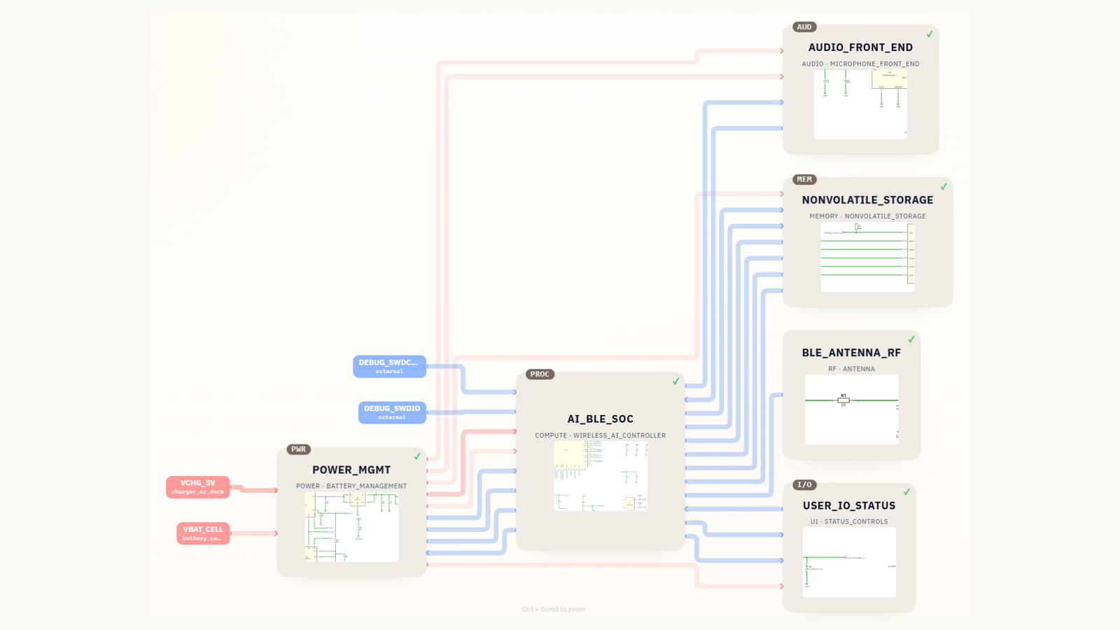
This guide uses a real SpeedUp-generated nRF52840 project with a GD5F1GQ5REYIGR SPI NAND device. The sheet is a concrete, editable KiCad starting point—not evidence that the memory and controller have been validated together. In particular, an electrical QSPI connection does not prove command-level compatibility. The exact memory data sheet, MCU peripheral documentation, software driver, layout, and prototype measurements still control the final design.
What Is QSPI?
Standard SPI normally transfers data over one controller-to-device line and one device-to-controller line. QSPI reuses the data pins as a wider bidirectional bus so selected operations can transfer two or four bits per clock. The interface still uses a serial clock and an active-low chip-select signal, but a transaction may contain phases with different bus widths: for example, a command on one line followed by an address or data phase on four lines.
That is why “quad” does not guarantee exactly four times the useful throughput. Command bytes, addresses, dummy cycles, memory-array latency, page boundaries, erase time, controller overhead, and the chosen read or program opcode all affect performance. The controller and memory must implement the same transaction format. The nRF52840 QSPI documentation, for example, exposes selectable single-, dual-, and quad-line read/write opcodes, address modes, SPI mode, clock frequency, page size, and deep-power-down settings.
External serial flash is commonly used for firmware images, assets, recorded data, logs, configuration, or over-the-air update staging. Infineon’s SPI serial flash overview summarizes the basic value proposition: nonvolatile storage with fewer pins and easier integration than a parallel memory interface. The engineering work begins when those general advantages must become an exact part, command set, power budget, footprint, and software stack.
SPI vs Dual SPI vs QSPI
| Interface mode | Data-path use | Typical schematic signals | Main design question |
|---|---|---|---|
| Standard SPI | One input and one output data line | CS_N, SCK, MOSI/SI, MISO/SO |
Does the required capacity and throughput fit a simple one-bit data path? |
| Dual SPI | Two bidirectional data lines during supported phases | CS_N, SCK, IO0, IO1 |
Do both devices support the same dual-output or dual-I/O command? |
| Quad SPI / QSPI | Four bidirectional data lines during supported phases | CS_N, SCK, IO0 through IO3 |
How are quad mode, opcodes, dummy cycles, drive strength, and reset states configured? |
A memory can support standard, dual, and quad transfers on the same package. The hardware should therefore name pins by their shared roles rather than assuming that IO2 is always write protect or IO3 is always hold. Those legacy functions may apply before quad mode is enabled, while the same pins become data lines during quad transfers. This dual use is also why reset-state pull-ups deserve deliberate attention.
QSPI Flash Pinout and Signal Roles
| Pin or net | Role | What to verify |
|---|---|---|
CS_N |
Selects the memory and frames each transaction | Reset default, inactive-high pull-up, minimum high time, boot behavior, and any shared-bus requirements |
SCK |
Clock from the controller | Supported frequency, SPI mode, duty cycle, drive strength, routing, and ringing |
IO0 |
Serial input in standard SPI; data bit in wider modes | Direction by transaction phase, logic levels, and controller pin mapping |
IO1 |
Serial output in standard SPI; data bit in wider modes | Power-up state, bus turnaround, logic levels, and controller pin mapping |
IO2 / WP_N |
Write-protect function in some states; data bit in quad mode | Required inactive level before quad mode and whether the exact device samples it at reset |
IO3 / HOLD_N |
Hold or reset-related function in some devices; data bit in quad mode | Required inactive level, reset behavior, and the exact part’s multifunction definition |
VCC, VSS, exposed pad |
Power and return | Operating range, I/O domain, current transients, local bypassing, thermal and assembly requirements |
Pin names are not a substitute for the exact data sheet. Two eight-pin memories can place similar labels on similar packages yet differ in voltage, command behavior, exposed-pad connection, reset function, quad-enable procedure, or package dimensions. Record the full orderable part number in the schematic and BOM, then build the firmware configuration from that part—not from a generic symbol.
Adding QSPI flash to an embedded product?
Describe the controller, memory capacity, voltage domain, read/write behavior, low-power states, and update strategy. Create a free account to start a reviewable, editable KiCad first draft.
Choose NOR or NAND Before Drawing the Circuit
“QSPI flash” describes an interface family, not a single memory architecture. Serial NOR and SPI NAND can both use one-, two-, or four-line transfers, but their internal organization and software responsibilities are different.
| Decision | Serial NOR tendency | SPI NAND tendency |
|---|---|---|
| Read model | Byte-addressable reads and often memory-mapped or execute-in-place use | Page-to-cache operation followed by cache read |
| Program and erase | Page program with sector or block erase | Page program through an internal cache with block-oriented erase |
| Media management | Usually a simpler software model | Bad-block handling and device-specific ECC/status behavior may matter |
| Typical selection pressure | Random reads, code or asset access, simpler controller integration | Higher density and data storage where the software stack supports NAND semantics |
Do not select NAND only because its capacity-per-package looks attractive, and do not select NOR only because the MCU peripheral is named QSPI. Start with the stored data, write pattern, retention, endurance, startup behavior, update strategy, file system, bad-block policy, and driver support. Then choose a device that the controller and software can operate correctly.
Check Controller and Memory Compatibility
The most important QSPI design gate is command-level compatibility. A schematic can connect the right six signals while the controller still cannot issue the memory’s required sequence. Compare the following items before committing the BOM:
- supported read, program, erase, status, reset, and deep-power-down commands;
- single-, dual-, and quad-line transaction formats for command, address, and data phases;
- 24-bit or 32-bit addressing and the resulting accessible capacity;
- page size, erase-block size, cache operations, and busy/status polling;
- quad-enable or feature-register setup after reset;
- SPI mode, maximum clock at the selected voltage, dummy cycles, and sampling delay;
- controller hardware limitations versus commands that can be sent through a general SPI peripheral; and
- driver, bootloader, file-system, and update-path support for the exact memory architecture.
Nordic specifies that the nRF52840 hardware QSPI block supports single-, dual-, and quad-line operations from 2 MHz to 32 MHz, EasyDMA transfers, and a defined set of read, page-program, erase, addressing, and power-down options. That feature list is not a blanket guarantee for every device marketed as QSPI. Compare those options with the exact memory command table and with the driver that will ship in the product.
If the hardware QSPI block does not match the required command sequence, a general SPI peripheral and a device-specific driver may sometimes be an alternative, but that changes throughput, CPU/DMA behavior, firmware scope, and boot or memory-mapped expectations. Make that architecture decision before layout rather than discovering it during board bring-up.
Design the Power, Pull-Ups, and Decoupling
Match the supply and I/O domains
Check the memory operating range against the actual rail over tolerance, startup, load transients, and temperature. Then check the controller output-high, output-low, and input thresholds against the memory I/O specifications. A nominally compatible 1.8 V label is not enough when the rail tolerance or device thresholds leave little margin.
External flash current is workload-dependent. Standby, continuous read, program, and erase conditions can have very different current profiles. Size the regulator and local reservoir from the data-sheet conditions that match the product’s behavior. If the device records audio, logs sensor data, or receives an update while the radio is active, test those concurrent loads rather than validating the memory in isolation.
Keep the memory deselected during reset
An inactive-high pull-up on CS_N can keep the flash deselected while the MCU pins are high impedance. Pull-ups on dual-purpose WP_N/IO2 and HOLD_N/IO3 can hold their legacy functions inactive before firmware enables wider transfers. The need and value depend on the exact devices, leakage, startup time, and bus topology; do not copy a resistor value without checking those conditions.
Place bypass capacitors at the package
Use the memory manufacturer’s recommended high-frequency bypass capacitor close to VCC and VSS, with a short return path. Add bulk capacitance when the power-distribution network and program/erase transients justify it. The schematic should show the intended values, but placement and loop geometry determine whether the high-frequency capacitor actually works.
Route QSPI Signals for a Reviewable Layout
QSPI is source-synchronous only in a broad functional sense; the receiving device samples signals against the clock generated by the controller. At higher edge rates, trace delay, skew, return discontinuities, stubs, crosstalk, package delay, and output drive strength can shrink the timing margin even when the nominal clock frequency seems modest.
- Keep
SCK,CS_N, andIO0throughIO3short and over a continuous reference plane. - Route the group together so the data paths do not have large relative length differences.
- Avoid layer transitions where possible; when transitions are necessary, maintain a nearby return path.
- Keep the bus away from switch nodes, inductors, antenna feeds, sensitive analog inputs, and high-current edges.
- Place optional source-series resistor footprints near the driving end only when signal-integrity analysis or measurement may require them.
- Use the controller’s documented drive-strength and recommended-pin guidance.
- Probe at the memory during bring-up, not only at the MCU pin.
Length matching is not a substitute for a timing budget. Derive acceptable skew and route length from the selected clock, device setup/hold requirements, output delay, board stackup, and controller sampling options. A compact memory placement near the MCU is usually more useful than chasing visually identical trace lengths across a large board.
Example From a Real SpeedUp Project

The project uses U6, a GD5F1GQ5REYIGR SPI NAND device, as local nonvolatile storage in a battery-powered nRF52840 recorder. The project’s BOM records a 1 Gbit device on a 1.7 V to 2.0 V supply. The GigaDevice GD5F1GQ5RE family page likewise identifies a 1.8 V-class, x1/x2/x4 SPI NAND family, while the exact orderable-part data sheet must control the final circuit and firmware decisions.
| Project item | Value or net | Engineering job |
|---|---|---|
| Flash | GD5F1GQ5REYIGR |
1 Gbit SPI NAND selected for local storage; exact command and driver support still require validation |
| Power | VDD_1V8 |
Matches the project’s memory voltage domain; tolerance and transient margin remain to be checked |
| Reset-state resistors | R18, R19, R20: 100 kΩ | Pull CS_N, IO2/WP_N, and IO3/HOLD_N high while controller pins may be high impedance |
| Local bypass | C36: 0.1 µF; C37: 4.7 µF | Provides high-frequency bypassing and local charge storage, subject to placement and data-sheet confirmation |
| Interface | STORAGE_QSPI_CS_N, SCK, IO0–IO3 |
Keeps the six controller-to-memory functions explicit across hierarchical sheets |
The good part of this sheet is its visibility: the supply, pull-ups, bypass capacitors, multifunction pins, and named bus are not hidden inside a generic “flash” block. The hierarchy carries STORAGE_QSPI_SCK, STORAGE_QSPI_CS_N, and STORAGE_QSPI_IO0 through STORAGE_QSPI_IO3 into the matching controller sheet. That makes the generated design discussable and editable. It also makes the unresolved question obvious. The GD5F1GQ5REYIGR is SPI NAND, while the nRF52840 hardware QSPI peripheral documents a specific transaction and opcode model. The team must compare the GD5F1GQ5 device data sheet, Nordic peripheral options, and chosen software stack before treating this pair as compatible.

For the full product prompt, architecture, audio path, power system, and other generated sheets, see the magnetic AI label microphone KiCad project. This QSPI guide owns the reusable storage-interface decisions; the project post owns the complete device example.
QSPI Flash Schematic Checklist
| Review area | What to confirm before layout |
|---|---|
| Use case | Capacity, read/write pattern, retention, update flow, boot role, and power-loss behavior |
| Memory architecture | NOR versus NAND, page and block organization, ECC, bad-block handling, and file-system needs |
| Controller support | Exact commands, bus widths, address mode, page size, status polling, deep power-down, and driver support |
| Power | VCC range, logic thresholds, regulator headroom, transient current, startup, and low-power states |
| Reset defaults | CS_N, WP_N/IO2, and HOLD_N/IO3 remain inactive until firmware configures the bus |
| Decoupling | Manufacturer-recommended bypass values and genuinely local placement/return paths |
| Pin mapping | Physical controller pins, package pins, shared functions, boot/debug conflicts, and recommended QSPI pins |
| Signal integrity | Clock rate, drive strength, route length, skew, reference plane, transitions, crosstalk, and optional damping |
| Footprint and sourcing | Exact WSON/DFN geometry, exposed pad, assembly rules, lifecycle, alternates, and second-source implications |
| Validation | Identification read, erase/program/readback, power interruption, temperature, endurance model, throughput, and sleep current |
Common QSPI Flash Circuit Mistakes
- Treating QSPI as a universal protocol. Matching signal names do not guarantee matching commands or memory semantics.
- Choosing capacity before architecture. A large NAND device is selected without a bad-block, ECC, driver, or file-system plan.
- Leaving multifunction pins undefined at reset. IO2 or IO3 activates a protection or hold function before quad mode is configured.
- Using the MCU’s maximum clock immediately. The memory, voltage, board timing, dummy-cycle setting, and sampling delay are not validated together.
- Checking VCC but not I/O thresholds. Both devices say 1.8 V, but worst-case logic margin is not demonstrated.
- Placing bypass parts far from the flash. The capacitors appear in the schematic but not in the high-frequency current loop.
- Using a generic eight-pin footprint. Body size, pad geometry, exposed pad, mask, paste, or pin-one orientation differs from the exact package.
- Ignoring power-loss behavior. An erase or page program is interrupted without a recovery or integrity strategy.
- Validating only a simple read. Program, erase, busy polling, sleep/wake, sustained transfers, and error handling remain untested.
- Calling a generated first draft production-ready. Firmware compatibility, layout timing, sourcing, assembly, reliability, and system tests are still open.
Prototype Validation Plan
Begin at low clock speed. Read the device identification and status registers, then confirm that the returned value matches the exact BOM part. Exercise reset and power cycling before testing higher-level storage. If the device requires feature-register configuration for quad mode, read back the setting rather than assuming the write succeeded.
Next, erase a known block or sector, program patterns that expose stuck bits and bus-order errors, and read them back through every intended transfer mode. Test page boundaries, maximum addresses, busy polling, timeouts, error bits, and recovery after an interrupted operation. For NAND, include bad-block and ECC/status handling in the validation plan. Save the exact firmware configuration, opcode mode, address width, clock, and dummy-cycle settings with the results.
Probe SCK, CS_N, and the data lines at the memory. Measure amplitude, overshoot, ringing, duty cycle, setup/hold margin, and relative timing while the bus runs at its intended clock. Repeat with the radio, audio path, charger, and other burst loads active. Finally, measure standby and active current, deep-power-down entry/exit, data integrity after power interruption, temperature behavior, and sustained application throughput.
How SpeedUp Fits
A useful product brief should say more than “add flash.” State what will be stored, required capacity, write frequency, retention, boot or update role, controller family, voltage domain, target throughput, sleep-current goal, file-system assumptions, and whether NOR or NAND is preferred. Those decisions give SpeedUp enough context to turn a behavior-level request into an electronics architecture, structured sheets, named interfaces, component and BOM context, and an editable KiCad first draft.
The output is a starting point for engineering, not the end of it. The team still verifies the exact memory command set, controller and driver compatibility, power integrity, reset states, layout timing, footprint, sourcing, firmware, reliability, and manufacturing plan. The embedded-system architecture guide shows how to define subsystem responsibilities before schematic capture, while the schematic-diagram guide explains how named interfaces make a multi-sheet design easier to continue.
Related Design Resources
- See the PDM microphone circuit guide for the matching audio subsystem in the same recorder architecture.
- Follow the product-brief-to-editable-KiCad workflow to see how requirements become structured engineering files.
FAQ
What does QSPI stand for?
QSPI usually means Quad Serial Peripheral Interface. It extends an SPI-style memory interface so supported transaction phases can use four bidirectional data lines instead of a single data path. The exact command, address, and data widths depend on the controller and memory configuration.
What is the difference between SPI and QSPI flash?
Standard SPI typically moves one bit per data line per clock using separate input and output signals. QSPI can use IO0 through IO3 together during supported read or program phases. QSPI can increase throughput, but only when both devices support the same opcodes, mode, dummy cycles, and timing. It does not by itself identify whether the memory is NOR or NAND.
How many pins does a QSPI flash interface need?
The active interface normally uses six signals: chip select, clock, and four data lines. The memory also needs power and ground, and some packages include an exposed pad. Before quad mode, IO2 and IO3 may act as write-protect and hold or reset-related pins, so their default states must be defined.
Can QSPI NAND replace QSPI NOR?
Not automatically. Both may expose an SPI or quad-width electrical interface, but NAND and NOR use different memory organizations, command flows, erase/program behavior, and software responsibilities. Confirm controller commands, driver support, bad-block and ECC handling, address model, and boot or memory-mapped requirements before substituting one architecture for the other.
Does the nRF52840 support QSPI flash?
Yes. Nordic documents a hardware QSPI peripheral with single-, dual-, and quad-line operations, configurable 2–32 MHz clocking, EasyDMA, and supported read, program, erase, address, and power-down settings. The exact external memory must still match those options and the chosen driver. A device described as QSPI is not automatically compatible.
Should CS, IO2, and IO3 have pull-up resistors?
A chip-select pull-up is commonly used to keep the memory deselected while the controller resets. Pull-ups on dual-purpose IO2/WP_N and IO3/HOLD_N can keep legacy protection or hold functions inactive before quad mode. Check the exact controller and memory data sheets, leakage, startup timing, and bus topology before choosing values.
Start Your QSPI Flash Project
Turn your storage and interface requirements into a reviewable QSPI schematic draft.
Use SpeedUp to turn the product requirements into structured schematic sheets and an editable KiCad first draft for engineering review. Create a free account to begin.