
Quick Answer
A schematic diagram is a functional map of an electrical or electronic circuit. It uses standardized symbols, reference designators, values, wires, net labels, and power symbols to show which components exist and how their pins connect. Unlike a physical wiring drawing or PCB layout, a schematic usually does not show the real size, position, or routing of the parts.
To read a schematic, begin with the power sources and return paths, identify the major functional blocks, and then follow one signal or power path at a time. To create one, start from product requirements and an electrical block diagram, define the power tree and interfaces, choose components, and convert each block into a readable circuit sheet. For a larger design, organize the schematic into named sheets whose interfaces are explicit at the top level.
A useful schematic must do more than look tidy. It should let another engineer answer four questions without guessing: what each circuit does, how power moves, how signals cross subsystem boundaries, and which assumptions still need validation.
Why Schematic Diagrams Matter
The schematic is where product behavior becomes electrical connectivity. A requirement such as “run from a rechargeable battery, wake on a button press, read a sensor, and update a display” is still too abstract for PCB design. The schematic turns that behavior into rails, components, nets, connectors, control signals, and documented boundaries.
That makes the schematic a shared engineering contract. Hardware engineers use it to inspect connectivity and component choices. Firmware engineers use it to find GPIO assignments, active levels, buses, interrupts, enables, and power states. Layout engineers use it to understand functional grouping and critical paths. Product, mechanical, sourcing, and test teams use it to find interfaces and unresolved constraints.
A visually polished diagram can still be a poor engineering artifact. If power domains are implicit, connectors have no return paths, net names change between pages, or a control signal has no defined owner, the drawing transfers uncertainty instead of knowledge. The goal is not decoration. It is a circuit description another person can trace and challenge.
The planning step comes first. The embedded system architecture guide explains how product behavior, operating states, power, compute, interfaces, and firmware responsibilities should be defined before detailed schematic capture.
Schematic Diagram vs Block Diagram vs Wiring Diagram
These drawings answer different questions. Treating them as interchangeable is a common source of incomplete handoffs.
| Drawing | Primary job | Usually shows | Usually omits |
|---|---|---|---|
| Electrical block diagram | Define system functions and relationships | Power, compute, sensing, communications, user I/O, major flows | Most components, pin-level connections, exact values |
| Schematic diagram | Define electrical components and connectivity | Symbols, pins, nets, labels, values, power domains, connectors | Physical board placement and routed copper |
| Wiring diagram | Guide physical installation or assembly | Connectors, terminals, cables, colors, harness or field connections | Detailed internal circuit behavior |
| PCB layout | Implement the circuit physically | Board outline, footprints, layers, traces, vias, copper areas, keepouts | A clean functional explanation of the circuit |
Have a product idea that needs a real schematic?
Describe the device behavior, power tree, functional blocks, interfaces, connectors, and operating states. Create a free account to start a reviewable, editable KiCad first draft.
A practical hardware workflow moves through these levels rather than choosing only one. The block diagram establishes scope, the schematic defines connectivity, the layout implements the circuit physically, and the wiring or assembly documentation explains external construction where required.
What a Useful Schematic Diagram Must Show
The exact content depends on the product, but every reviewable schematic needs a consistent information model. Use this framework before worrying about visual styling.
| Area | What readers should be able to identify | Typical evidence |
|---|---|---|
| Function | Why the circuit exists and which subsystem owns it | Sheet name, section label, short design note |
| Components | Which parts are used and how each instance is identified | Symbols, reference designators, values, part numbers, footprints when known |
| Connectivity | Which pins are electrically connected | Wires, junctions, net labels, bus labels, sheet pins |
| Power | Where energy enters, how rails are created, and what returns to ground | Input source, protection, regulators, rail names, enables, grounds, decoupling |
| Interfaces | How subsystems communicate and which side owns each signal | I2C, SPI, UART, USB, CAN, interrupts, reset, enables, connector pinouts |
| Assumptions | Which decisions are provisional or owned outside the schematic | Notes for firmware behavior, mechanical limits, sourcing choices, layout constraints |
Symbols and reference designators
A symbol represents an electrical function, not the physical appearance of the package. Reference designators distinguish instances: resistors commonly use R, capacitors C, diodes D, integrated circuits U, connectors J, and switches SW. The symbol and reference tell you what the part does and which specific instance you are discussing; the footprint later determines how that part lands on a board.
Wires, junctions, and net labels
A drawn wire indicates an electrical connection between endpoints. A junction marker clarifies a branch. A net label names connectivity without forcing a long line across the page. Good names such as SENSOR_I2C_SDA, DISPLAY_RST_N, or BATTERY_LOW_N carry more engineering meaning than repeated anonymous wires.
Power symbols are connectivity, not decoration
A rail label such as VBAT, 5V, 3V3, or 1V8 should refer to a defined domain. The schematic should show where the rail comes from, what enables it, which loads use it, and which ground or return path completes the circuit. Do not let a familiar power symbol hide an undefined source or an incompatible voltage domain.
How to Read Schematics Step by Step
Trying to understand every symbol at once makes a large schematic feel harder than it is. Read it in passes.
1. Read the title block and sheet hierarchy
Confirm the project, sheet name, revision, and page position before interpreting the circuit. In a multi-sheet design, open the root or top-level sheet first. It should tell you which subsystems exist and how to enter the detailed pages.
2. Find the power source and rail conversions
Start at the battery, USB input, adapter, or external supply. Follow protection, switching, regulation, and rail-distribution stages. Record the expected voltage of each rail, whether it is always on or controlled, and which signals report power status. This exposes hidden assumptions early because every active circuit depends on the power tree.
3. Identify the controller and functional blocks
Find the MCU, processor, programmable logic device, or analog control core. Then identify sensors, radios, displays, storage, actuators, user controls, and external connectors. Give each block a one-sentence job. If you cannot explain why a block exists, the diagram needs better structure or documentation.
4. Trace one path at a time
Choose a specific behavior and trace only the relevant path. For example: a button changes state, the MCU sees an input, firmware enables a display rail, and an SPI interface updates the screen. Then trace a different job, such as an I2C sensor measurement. This behavior-first method is faster than reading reference designators in numerical order.
5. Check active levels, directions, and boundaries
A suffix such as _N often indicates an active-low signal, but confirm the actual device behavior. Identify whether a signal is an input, output, bidirectional bus, clock, interrupt, reset, or enable. At every connector or sheet boundary, verify that the name, voltage domain, return path, and ownership remain clear.
6. Separate what the schematic proves from what it does not
A schematic can show intended connectivity and component context. It does not prove that a regulator is thermally adequate, an antenna is placed correctly, a high-speed interface is routed well, firmware handles every state, a footprint matches the supplier part, or the assembled product satisfies safety and compliance requirements. Record those as downstream validation tasks instead of assuming the drawing answers them.
How to Create a Schematic Diagram From a Block Diagram
Do not begin by dropping a favorite MCU onto an empty page. Create the circuit from product decisions in a controlled sequence.
1. Write measurable product requirements
Describe power source and runtime, charging or external power, required sensing and control, wired and wireless interfaces, display and user input, operating states, environmental limits, enclosure constraints, preferred components, service access, and expected engineering outputs. Separate hard requirements from preferences and proposed solutions.
2. Draw the electrical block diagram
Create one block for each meaningful subsystem. Connect the blocks with named power or signal flows. At this stage, the question is whether the proposed architecture can support the product behavior—not whether every capacitor value has been selected.
3. Build the power tree first
List every input and generated rail. Estimate normal and peak loads, define which rails can be switched, and document startup, shutdown, and fault assumptions. Power decisions influence component choice, connectors, firmware sequencing, thermal behavior, and the sheet hierarchy, so they should not be left until the end.
4. Choose components with their surrounding circuits
A component selection is not only a part number. Capture the required decoupling, clocking, reset, boot configuration, protection, biasing, sensing, connectors, programming access, and support parts described by the manufacturer. Record which values are calculated, which come from a reference design, and which remain assumptions.
5. Define each interface before drawing long wires
For every connection between blocks, define signal names, direction, voltage domain, pull-ups or termination where relevant, connector pins, cable assumptions, and firmware ownership. This turns an architectural arrow into a reviewable electrical contract.
6. Draw one functional sheet at a time
Keep related components together, prefer a consistent left-to-right flow where practical, label rails and interfaces clearly, and add short notes where the circuit alone cannot explain intent. Revisit the root sheet after each module so the system view stays synchronized with the detailed design.
How to Organize Multi-Sheet Circuits in KiCad
A small circuit can fit on one page. A product with power management, compute, sensors, communications, storage, display, and user I/O usually becomes easier to review when those concerns are separated. The goal is not to maximize the number of sheets; it is to make each sheet responsible for a coherent function.
KiCad’s current Schematic Editor documentation describes top-level and hierarchical sheets, global labels, hierarchical labels, and sheet pins. Global labels connect matching names across the schematic. Hierarchical labels and matching sheet pins make a child sheet’s interface visible in its parent. That difference is important: a controlled sheet interface is easier to inspect than a design connected everywhere by invisible global scope.
Choose sheet boundaries by responsibility
Good sheet names describe stable functions: POWER_INPUT, COMPUTE_WIRELESS, SENSOR_INTERFACE, DISPLAY_SUBSYSTEM, or USER_IO. Avoid arbitrary divisions such as “Page 2” or “Miscellaneous.” A reviewer should be able to predict what belongs inside a sheet from its name.
Make the top level an interface map
The root sheet should show the product’s functional decomposition and the signals that cross boundaries. It does not need to repeat internal component detail. A good top level lets a reviewer see the power inputs, generated rails, buses, enables, interrupts, resets, and connector-facing signals before opening any child sheet.
Use names that carry meaning across pages
Name an interface for its job, not for the page where it happens to appear. DISPLAY_SPI_SCK is more stable than PAGE3_CLK. Use one spelling and active-level convention throughout the project. When a child sheet changes, update the parent interface at the same time.
Example From a Real SpeedUp Project
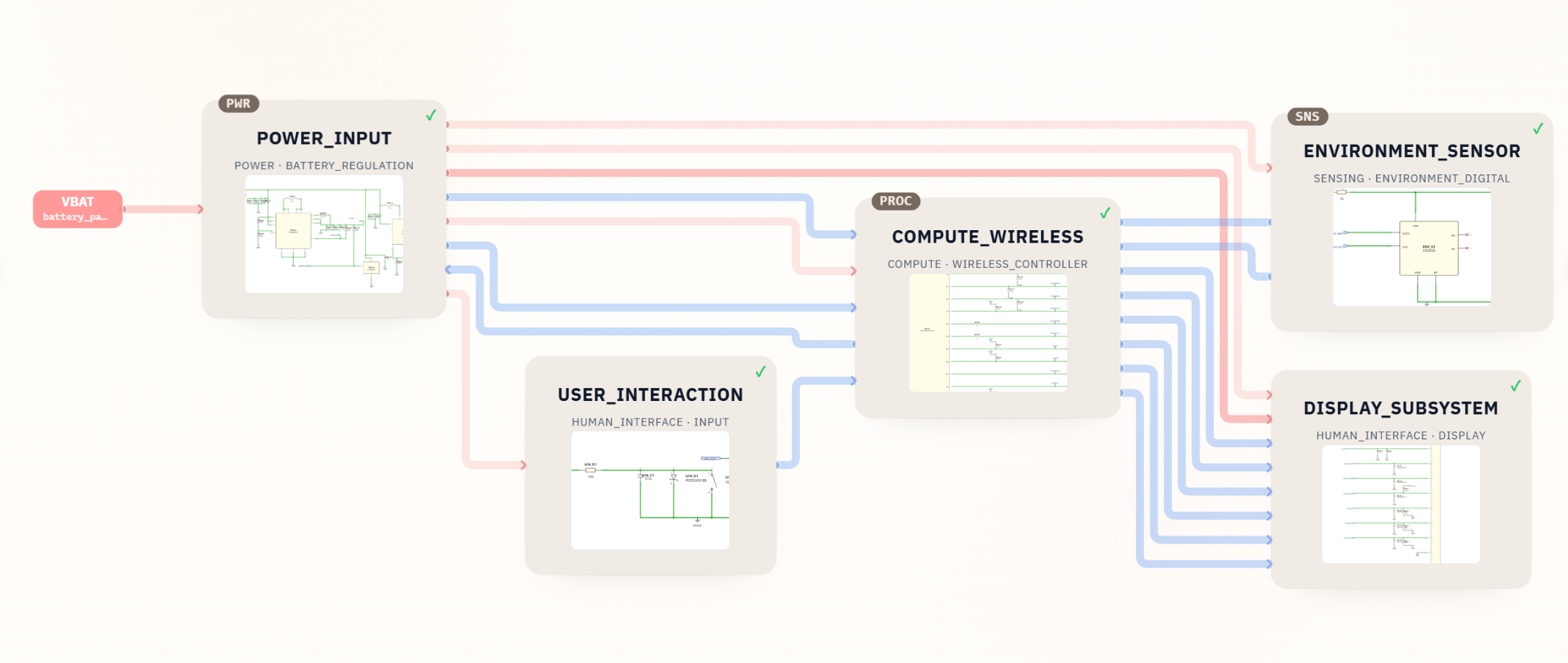
The real Desktop Robot KiCad project shows how an electrical block diagram can become a structured schematic package. The source project contains a root schematic plus five named module sheets: POWER_INPUT, COMPUTE_WIRELESS, DISPLAY_SUBSYSTEM, ENVIRONMENT_SENSOR, and USER_INTERACTION.

The root page immediately reveals the system structure. VBAT enters the power sheet. The power block exposes SYS_3V3, a controlled display rail, battery status, and power-good signals. The compute sheet connects to the display over named SPI and control signals, to the environmental sensor over I2C, and to the user-input sheet through an event signal.
The package also contains the KiCad project file, local symbol and footprint libraries, and a BOM with 39 line items and 75 placed quantities. That does not make the design production-ready, but it makes the architecture concrete enough for an engineer to open, trace, edit, and review. Readers who want to see the broader prompt-to-file workflow can continue with the KiCad schematic generator guide.
Common Schematic Diagram Mistakes
- Drawing physical placement instead of functional connectivity. A schematic should optimize for understanding the circuit. The PCB layout handles real placement and routing.
- Starting with a preferred component before requirements. This can force the product around an MCU, regulator, sensor, or radio that does not fit the actual power, interface, package, or lifecycle needs.
- Hiding the power tree behind repeated symbols. Every rail still needs an identifiable source, operating range, control behavior, and return path.
- Using long anonymous wires or vague labels. Names should reveal interface purpose, active level, and domain without requiring the reviewer to memorize page coordinates.
- Putting the complete product on one crowded sheet. A single page is not automatically simpler. Once the design contains several stable subsystems, clear sheet boundaries make reviews more focused.
- Using global labels for every cross-page connection. Broad scope can make dependencies harder to see. Prefer explicit parent-child interfaces when the design is hierarchical.
- Copying a reference circuit without product context. A vendor example may support one component, but it does not define the complete product’s power states, connectors, mechanical limits, firmware behavior, sourcing, or validation plan.
- Treating a generated schematic as a finished product. A first draft still needs engineering review of parts, symbols, footprints, power, RF, safety, layout, firmware, sourcing, test, compliance, and manufacturing requirements.
How SpeedUp Fits
SpeedUp helps move from a plain-language product brief to an electronics architecture and a structured schematic draft. Supported projects can include named functional sheets, component context, BOM information, local libraries, and an editable KiCad project rather than only a static image. The AI circuit schematic generator guide explains that product path in more detail.
The result should be treated as a first engineering draft for review. Engineers still decide whether the architecture is complete, verify the electrical design and manufacturer guidance, validate symbols and footprints, develop the PCB layout and firmware, manage sourcing, plan tests, and address safety, compliance, and manufacturing before release.
Related Project Examples
- How to review an AI-generated KiCad schematic — a systematic follow-on once the first draft exists.
- Temperature and humidity sensor KiCad project — a smaller three-sheet example covering power, sensing, and control/display.
FAQ
What is a schematic diagram?
A schematic diagram is a symbolic representation of a circuit’s components and electrical connections. It explains circuit function and connectivity without trying to reproduce the physical appearance or placement of the parts.
How do I read schematics as a beginner?
Start with the title and top-level organization, find the power source and ground, identify the controller and main functional blocks, and trace one behavior at a time. Learn common symbols gradually and rely on reference designators, values, and net names instead of trying to memorize the whole page.
How do you create a simple schematic diagram?
Define the required behavior and power source, draw a small block diagram, select the main components and their support circuits, name the rails and interfaces, and then draw the connections in a schematic editor. Add reference designators, values, notes, and connectors so another person can review the result.
What is the difference between a block diagram and a schematic?
A block diagram shows system functions and the relationships between them. A schematic implements those functions with specific components, pins, values, nets, and power connections. One block may become one circuit sheet or several detailed sheets.
Can AI create a schematic diagram?
AI-assisted tools can help turn a detailed product brief into an initial architecture and editable schematic draft. The usefulness of the result depends on the quality of the requirements and the available component context. A qualified engineer must still review and validate the design before it is used for a physical product.
Create Your Schematic Starting Point
Turn the product idea into organized schematic sheets and an editable KiCad project.
Use SpeedUp to turn the product requirements into structured schematic sheets and an editable KiCad first draft for engineering review. Create a free account to begin.
Comments
No comments yet.
Leave a Reply