
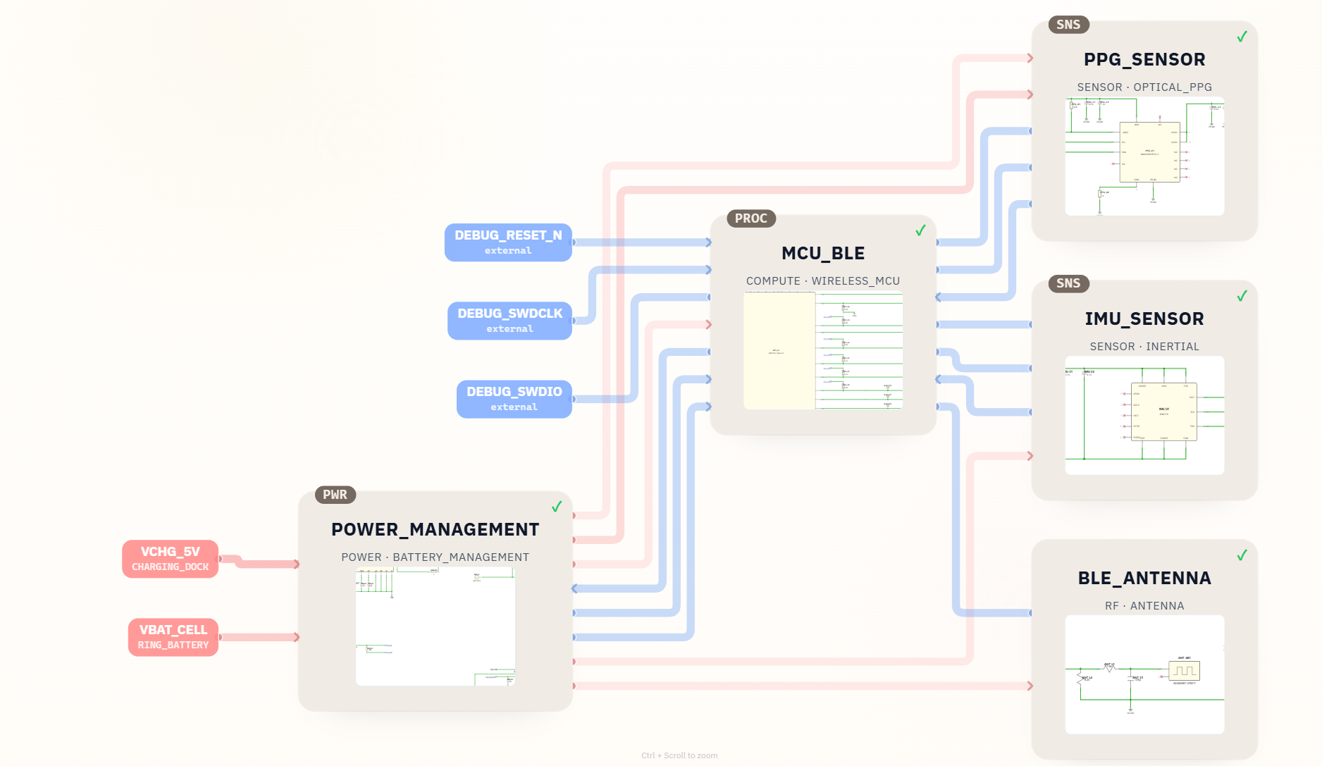
This project shows how SpeedUp turned a smart ring idea into an editable KiCad schematic for sleep and heart-rate monitoring. From one prompt, SpeedUp generated a wearable architecture with nRF52832 BLE compute, MAX30102 optical PPG sensing, BMI270 inertial sensing, battery power management, debug access, five hierarchical sheets, and a BOM for engineering review.
This is a first engineering draft for review, not a production-ready smart ring reference design. The source package contains project.kicad_pro, the top-level project.kicad_sch, five module sheets, a 44-line-item BOM, and local symbol and footprint libraries. It does not include a PCB layout.
Project Summary
| Field | Details |
|---|---|
| Project | Smart ring for sleep and heart-rate monitoring |
| Input | Natural-language prompt |
| Output | Editable KiCad 10 schematic project, BOM, and local symbol/footprint libraries |
| Key modules | POWER_MANAGEMENT, MCU_BLE, PPG_SENSOR, IMU_SENSOR, BLE_ANTENNA |
| Main components | nRF52832 BLE MCU, MAX30102 PPG sensor, BMI270 six-axis IMU |
| Included files | project.kicad_pro, top-level and five hierarchical schematic sheets, XLSX BOM, 13 symbol libraries, 23 footprint files, and project-evidence images |
| Next engineering work | BOM and footprint review, PCB or rigid-flex layout, firmware, Gerbers, mechanical design, optical validation, and RF testing |
| Status | First engineering draft for review |
The Prompt
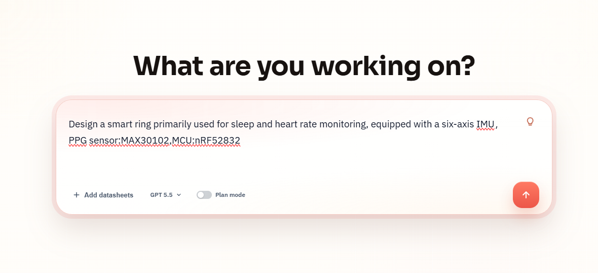
The project starts with a compact wearable-device request:
Design a smart ring primarily used for sleep and heart rate monitoring, equipped with a six-axis IMU, PPG sensor:MAX30102,MCU:nRF52832
What SpeedUp Generated
SpeedUp turned the prompt into a structured smart ring circuit design with:
- A block diagram for the wearable architecture.
- An editable KiCad project with
project.kicad_pro, a top-levelproject.kicad_sch, and five hierarchical schematic sheets. - A
POWER_MANAGEMENTblock for charging, battery, system power, 1.8 V rail, and PPG LED power. - An
MCU_BLEblock usingNRF52832-QFAA-G-Rwith clocks, decoupling, I2C, interrupts, and SWD/debug connections. - A
PPG_SENSORblock aroundMAX30102EFD+Tfor optical heart-rate and SpO2-style sensing. - An
IMU_SENSORblock aroundBMI270for motion and sleep-context sensing. - A
BLE_ANTENNAblock in the generated architecture. - A downloadable source package with the KiCad project, 44-line-item BOM, 13 local symbol libraries, 23 local footprint files, and the prompt, block diagram, and top-level schematic images.
Want to create a wearable sensor like this?
Describe your own wearable sensor requirements and create a free account to start a reviewable engineering draft.
Project Architecture
The generated design follows a common smart ring structure: a low-power BLE MCU coordinates sensors, a compact battery power tree feeds the electronics, and optical/inertial sensors provide the core health and motion signals.
POWER_MANAGEMENT: connectsVCHG_5Vfrom a charging dock,VBAT_CELLfrom the ring battery, system power, 1.8 V logic power, battery monitoring, charge status, and PPG LED power.MCU_BLE: handles BLE compute, I2C sensor communication, PPG LED control, sensor interrupts, reset, SWD debug, clocks, and RF output.PPG_SENSOR: connects the MAX30102 optical sensor to I2C, interrupt, logic power, and dedicated LED power.IMU_SENSOR: connects a BMI270 six-axis inertial sensor to I2C and interrupt lines.BLE_ANTENNA: routes the BLE RF output toward the antenna path shown in the architecture.
This page is useful for people searching for smart ring circuit design because it shows the engineering shape of the design, not only the product concept. It also shows the review gaps that still matter before a ring can become a board-ready or product-ready design.
Top-Level KiCad Schematic Output
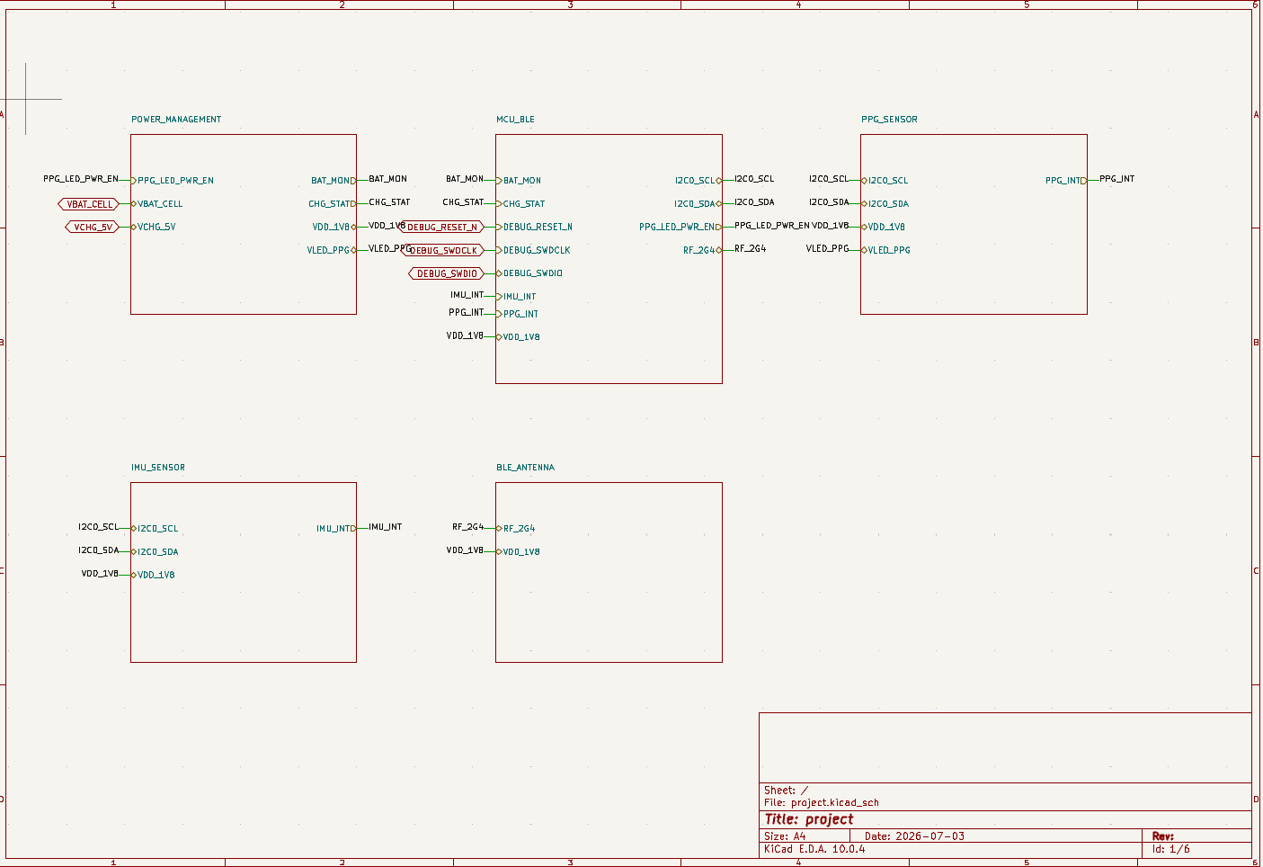
The top-level project.kicad_sch connects POWER_MANAGEMENT, MCU_BLE, PPG_SENSOR, IMU_SENSOR, and BLE_ANTENNA. Engineers can open and edit these sheets directly in KiCad 10; the package does not include a .kicad_pcb file.
nRF52832 BLE MCU Subsystem
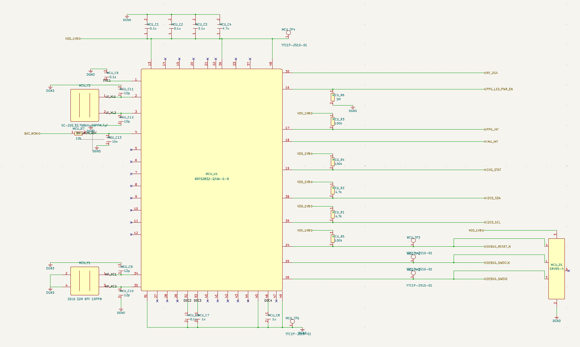
The MCU block is the control center for the ring. It connects to the PPG and IMU sensors over I2C, receives sensor interrupt signals, controls PPG LED power, exposes SWD clock/data and reset for debug, and routes RF_2G4 toward the BLE antenna block.
This subsystem still needs review for nRF52832 pin assignments, low-power sleep states, interrupt wake behavior, RF layout, crystal loading, decoupling placement, firmware boot/debug requirements, and whether the selected pins are practical in a very small ring PCB or rigid-flex layout.
MAX30102 PPG Sensor Subsystem
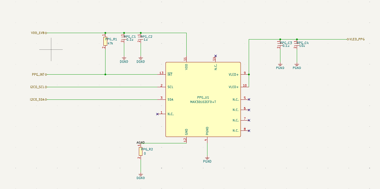
The PPG sensor is the most product-defining part of this smart ring concept because it supports heart-rate and sleep-related signal collection. The generated circuit separates logic power from the PPG LED supply and exposes PPG_INT, I2C0_SCL, I2C0_SDA, and VLED_PPG.
Before layout, the optical design needs serious human review. A real smart ring must validate sensor placement against the finger, LED current and thermal behavior, ambient-light rejection, mechanical window design, skin contact pressure, motion artifacts, and algorithm assumptions. The schematic is a starting point, not a guarantee of clinical-quality measurement.
BMI270 IMU Subsystem
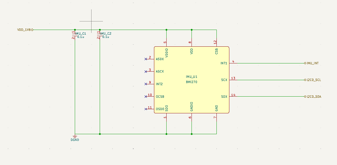
The IMU gives the ring motion context for sleep tracking, activity detection, and sensor fusion. The generated schematic keeps the IMU interface simple: shared I2C, local decoupling, chip-select handling, and IMU_INT back to the MCU.
Review this block for I2C address conflicts, interrupt polarity, standby current, sensor sampling modes, mechanical orientation, vibration exposure, and whether the IMU placement inside the ring matches the intended algorithm model.
Power Management Subsystem
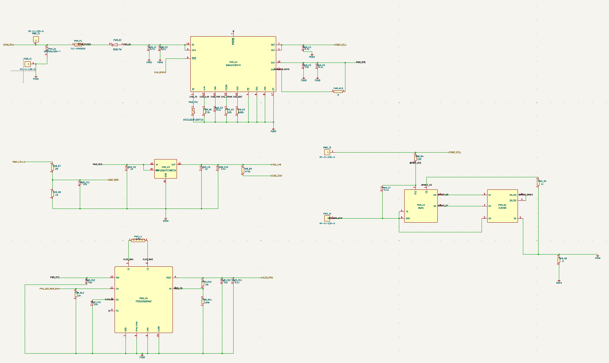
Power is the hardest part of a compact smart ring design. The generated power sheet gives a reviewable starting point for charging, battery monitoring, system power, and sensor LED power. It also exposes the product constraint that will dominate the final design: the electronics must fit inside a tiny wearable while staying cool, safe, and low power.
This section needs review for battery chemistry, charger IC settings, charge current, protection, thermal rise on the finger, magnetic charging contacts, leakage current, 1.8 V rail budget, PPG LED current peaks, battery gauge accuracy, and sleep-mode current.
BOM and Engineering Handoff
The included XLSX BOM contains 44 line items and 86 placed quantities. It provides MPN, package, footprint, description, and notes fields for sourcing and handoff review, but every part, land pattern, rating, and alternate still needs engineering validation.
Before using this design for layout, engineers should prepare:
- A controlled schematic revision and design-review record.
- BOM review with validated MPNs, quantities, packages, land patterns, alternates, and sourcing notes.
- PCB layout or rigid-flex layout.
- Gerbers, drill files, pick-and-place, and assembly drawings.
- Firmware project, boot/debug plan, and BLE power profile.
- Mechanical stack-up, battery selection, antenna strategy, optical window, and charging dock definition.
What Still Needs Human Review
This project is intended as a first engineering draft. Before treating it as a board-ready smart ring design, review:
- Ring mechanical constraints, including PCB shape, rigid-flex strategy, battery volume, charging contacts, and sensor window placement.
- PPG optical stack, LED current, photodiode alignment, finger contact pressure, ambient-light shielding, and skin-safety assumptions.
- Power budget for BLE advertising/connection, PPG LED pulses, IMU sampling, sleep tracking, and deep sleep.
- nRF52832 RF layout, antenna detuning by the finger, matching network, ground clearance, and enclosure effects.
- Battery charging safety, thermal behavior, protection, leakage current, and charge-contact reliability.
- I2C pull-ups, voltage levels, sensor addresses, interrupt behavior, and wake-from-sleep firmware logic.
- Footprints, land patterns, assembly tolerances, component availability, and wearable manufacturing constraints.
- Regulatory, EMC, biocompatibility, privacy, and medical-claim boundaries.
Related SpeedUp Projects and Guides
- AI Schematic Generator for KiCad Circuit Projects
- Schematic Review Checklist Before PCB Layout
- Temperature and Humidity Sensor KiCad Project
FAQ
Is this smart ring design production ready?
No. This is a first engineering draft generated for review and iteration. It needs BOM review, PCB or rigid-flex layout, firmware, mechanical design, optical validation, RF testing, safety checks, and manufacturability work before production.
What files are included in the generated package?
The ZIP includes project.kicad_pro, the top-level project.kicad_sch, five hierarchical schematic sheets, a 44-line-item / 86-placed-quantity XLSX BOM, 13 symbol libraries, 23 footprint files, and prompt, block-diagram, and top-level-schematic images. No .kicad_pcb is included.
How is a smart ring powered?
This generated design uses a ring battery input, a 5 V charging-dock input, charge management, system power, a 1.8 V rail, and a PPG LED power path. A production design still needs battery selection, charger settings, thermal validation, protection, and charge-contact design.
What is the smart ring structure in this design?
The design is organized around power management, a BLE MCU, optical PPG sensing, inertial sensing, and BLE antenna routing. Those blocks match the main technical jobs of a health-monitoring smart ring: power, compute, sensing, wireless communication, and bring-up/debug access.
Does this smart ring detect AFib or provide medical diagnosis?
No. The generated circuit is only an engineering draft for sleep and heart-rate monitoring concepts. AFib detection or medical diagnosis would require validated sensors, signal-processing firmware, clinical testing, regulatory review, and careful claims control.
Can I generate a similar wearable circuit from my own prompt?
Yes. SpeedUp is designed to turn a natural-language hardware idea into structured engineering artifacts such as architecture diagrams, schematic screenshots, subsystem details, and review packages that engineers can inspect and refine.
Download the Smart Ring KiCad Source
Use this smart ring ZIP as a review starting point for the generated editable KiCad schematic. It includes the project and schematic source, five module sheets, the BOM, local symbol and footprint libraries, and project-evidence images; add a reviewed PCB or rigid-flex layout, firmware, mechanical CAD, optical validation, RF tuning, Gerbers, production tests, and manufacturing-release documentation before treating it as a complete engineering handoff.
Create Your Own Wearable Sensor Project
Turn your own wearable sensor brief into reviewable engineering artifacts.
Use SpeedUp to generate structured schematic sheets and an editable KiCad project for engineering review. Create a free account to begin.
Comments
No comments yet.
Leave a Reply