
Quick Answer
A snubber circuit controls voltage overshoot and ringing caused by parasitic inductance and capacitance when current switches quickly. For high-frequency MOSFET or rectifier ringing, a series RC network placed directly across the ringing device or switching node is a common starting point. Do not choose the resistor and capacitor from a generic table: measure the unsnubbed ringing, estimate the parasitic L and C, calculate starting values, then tune them on the real PCB.
A useful measurement-based starting method is to measure the original ring frequency f0, add a known test capacitor C1, measure the shifted frequency f1, and calculate the parasitic network. Start with Csnub ≈ 3C0 and Rsnub ≈ √(L/C0). Verify peak voltage, resistor loss, device temperature, switching loss, EMI, and behavior across voltage, load, temperature, and component tolerances before production.
Why Snubber Circuits Matter
A schematic may show an ideal MOSFET, diode, transformer, motor winding, or relay contact, but the assembled circuit contains trace inductance, package inductance, transformer leakage inductance, MOSFET output capacitance, diode junction capacitance, winding capacitance, and connector or cable parasitics. When current changes quickly, those unintended elements exchange energy and create an underdamped oscillation.
The visible symptoms include drain-voltage overshoot, rectifier ringing, switch-node oscillation, false turn-on through the Miller capacitance, noisy current sensing, radiated and conducted EMI, contact arcing, or device avalanche stress. The first design action is still to reduce the parasitic loop with better component placement, return paths, package selection, and switching-loop geometry. A snubber dissipates remaining resonant energy; it should not be used to conceal an avoidable high-inductance layout.
Texas Instruments describes the ringing as an LC tank formed by real component and PCB parasitics and shows a measurement-based way to calculate an RC starting point in its seven-step RC snubber procedure. The method is useful because the parasitic values that matter are often not known accurately from the schematic alone.
What Is a Snubber Circuit?
A snubber is a passive or active network that changes a circuit’s transient response. The right topology depends on whether the problem is repetitive high-frequency ringing, a unidirectional leakage-inductance spike, contact arcing, gate oscillation, or an absolute-voltage clamp requirement. “Add a snubber” is not a complete design instruction until the ringing path, protected device, energy, frequency, and acceptable loss are defined.
| Network | Typical job | Main trade-off |
|---|---|---|
| C snubber | Absorbs transient energy and reduces voltage slew or overshoot. | Large repetitive charge/discharge current and possible oscillation with its own path inductance. |
| Series RC snubber | Damps a measured high-frequency LC ring across a MOSFET, diode, switch node, winding, or load. | Resistor dissipates energy every switching cycle; capacitor increases switching current. |
| RCD clamp/snubber | Steers and dissipates unidirectional leakage-inductance energy, common in flyback and other inductive converters. | Diode recovery, clamp voltage, ripple, average loss, and layout all require topology-specific calculation. |
| TVS or avalanche clamp | Limits voltage above a defined threshold. | May clamp the peak without critically damping the underlying oscillation; pulse and repetition ratings matter. |
| Gate resistor or ferrite | Controls gate-loop ringing and switching edge rate. | Slower switching can increase MOSFET loss; it is not a substitute for damping a drain or switch-node resonance. |
Designing a switching-power or motor circuit?
Describe the power stage, switching devices, loads, ringing measurements, safety constraints, and test requirements. Create a free account to start a reviewable, editable KiCad first draft.
A flyback diode is also not automatically an RC snubber. It provides a recirculation path for inductive current in many low-side DC loads, while an RC network damps an oscillatory transient. The flyback diode polarity, placement, and sizing guide explains when that simpler clamp is the correct first protection element.
Find the Ringing Loop Before Choosing Values
Measure the node and identify the transition that creates the oscillation. A waveform that appears after MOSFET turn-off may come from drain-loop inductance and Coss, transformer leakage inductance and rectifier capacitance, or a probe ground lead. A phase-node waveform can include commutation behavior, cable reflection, common-mode coupling, dead-time effects, and the motor’s impedance. The same-looking ringing can require a different network and reference node.
- Reproduce the worst relevant operating condition with a current-limited, protected setup.
- Use a low-inductance probe connection or a correctly rated differential probe. Verify that the waveform is not created by the probe loop.
- Record bus voltage, load current, switching frequency, gate resistance, temperature, probe type, and measurement point.
- Measure ring frequency, peak voltage, decay, and the switching event that starts it.
- Sketch the high-frequency current loop and identify which device voltage or current needs protection.
Before adding damping parts, minimize the gate and source-path inductance, shrink the gate-loop area, keep the power commutation loop compact, and avoid unnecessary vias. Also distinguish a drain-to-source RC snubber from a gate resistor: they act on related but different resonant paths.
How to Calculate Starting RC Snubber Values
The following workflow adapts the TI frequency-shift method for a series RC network across the ringing device. It produces starting values, not final production values. Use it only when the test capacitor can be added safely at the intended node and the measurement setup is appropriate for the circuit voltage and energy.
1. Measure the original ringing frequency
Measure the unsnubbed ringing frequency f0 with the shortest practical probing loop. Do not derive it from switching frequency: the ring is a parasitic resonance and may be tens or hundreds of megahertz even when the converter switches at kilohertz.
2. Add a known test capacitor and measure again
Add a known capacitor C1 directly across the same two nodes intended for the snubber and measure the new frequency f1. The capacitor must have adequate voltage, pulse-current, dielectric, and safety rating. A meaningful downward frequency shift makes the calculation less sensitive to measurement error.
3. Calculate the parasitic capacitance and inductance
m = f0 / f1C0 = C1 / (m² - 1)L = (m² - 1) / ((2πf0)² × C1)
C0 is the effective parasitic capacitance participating in the measured ring and L is the corresponding loop inductance. These are operating-point estimates because semiconductor capacitance changes with voltage and the active loop may change with state.
4. Calculate starting snubber values
Csnub ≈ 3 × C0Rsnub ≈ √(L / C0)
Choose nearby standard values and reserve more than one component footprint when practical. The calculated resistance is a damping starting point, while the capacitor determines how much of the transient energy the network captures. More capacitance usually reduces the spike further but increases current and dissipation.
Worked Example: 50 MHz Ringing
Assume a protected bench measurement shows f0 = 50 MHz. Adding C1 = 470 pF across the ringing device shifts the frequency to f1 = 35.4 MHz.
m = 50 / 35.4 ≈ 1.414C0 = 470 pF / (1.414² - 1) ≈ 470 pFL ≈ 21.6 nHCsnub ≈ 3 × 470 pF = 1.41 nF, so 1.5 nF is a reasonable bench starting valueRsnub ≈ √(21.6 nH / 470 pF) = 6.8 Ω
For an illustrative 48 V swing at 100 kHz, the common first-pass loss estimate P ≈ C × V² × f gives approximately 1.5 nF × 48² × 100 kHz = 0.35 W. That is not permission to fit a 0.5 W generic resistor. Waveform shape, pulse energy, duty, voltage dependence, switching events per cycle, airflow, ambient temperature, PCB copper, and resistor pulse rating all matter. ROHM shows the same loss relationship in its DC-DC snubber loss example and emphasizes the efficiency trade-off.
Select the Resistor and Capacitor for Real Stress
The resistor must survive both average heating and repetitive pulses. Check working voltage, pulse-energy curves, overload rating, package inductance, temperature coefficient, and derating—not only the printed wattage. Several series or parallel resistors may distribute voltage, power, and inductance, but the new layout still has to keep the snubber loop tight.
The capacitor needs margin for the real transient voltage, repetitive RMS or pulse current, temperature, bias dependence, dielectric loss, and expected lifetime. Small C0G/NP0 ceramic capacitors can be attractive for low-value high-frequency damping. Larger high-voltage networks may require pulse-rated film capacitors or a topology-specific part. For offline circuits, safety-class requirements depend on whether the capacitor is across line, line-to-earth, across reinforced isolation, or entirely inside the primary switching loop; do not substitute an ordinary capacitor where an approved safety component is required.
Check the capacitor’s effective capacitance at the actual DC bias. A nominal high-K ceramic can lose a substantial fraction of its value at voltage. Also compare capacitor ESR and ESL with the intended damping path: a physically large part or long trace can add enough inductance to weaken the network at the measured ring frequency.
Snubber Placement and PCB Layout
Place the series RC network across the two nodes that form the measured resonance and keep the entire high-frequency path short and compact. For a drain-to-source MOSFET snubber, route directly to the power terminals or Kelvin-connected copper near the device—not to a distant bus connector or broad net with shared inductance. For a rectifier snubber, close the loop around the diode and relevant winding or switch node. ROHM’s snubber design application note explicitly recommends placing the network as close as possible to the MOSFET and minimizing snubber-path inductance.
| Layout check | What to verify | Why it matters |
|---|---|---|
| Loop area | Shortest path from device terminal through C and R back to the other terminal | Added inductance prevents the network from absorbing the high-frequency transient |
| Reference node | Power ground, switch return, phase, chassis, or isolated primary node is intentionally chosen | A convenient ground symbol may inject common-mode current into the wrong domain |
| Thermal path | Resistor copper, spacing, nearby heat sources, enclosure airflow, and touch temperature | Average dissipation can be modest while the local resistor runs too hot |
| Voltage spacing | Clearance, creepage, coating assumptions, pollution degree, and isolation boundary | The snubber sits on the transient it is meant to suppress |
| Probe access | Safe, low-inductance test points for the protected voltage and relevant current | Production tuning and fault analysis need repeatable measurements |
| Options | DNP footprints and alternative R/C sizes without long stubs | The final value normally changes after first-board measurement |
After the schematic values are reviewed, use the KiCad schematic-to-PCB layout checklist to preserve these current-loop, return-path, spacing, placement, and test-access constraints in the routed board.
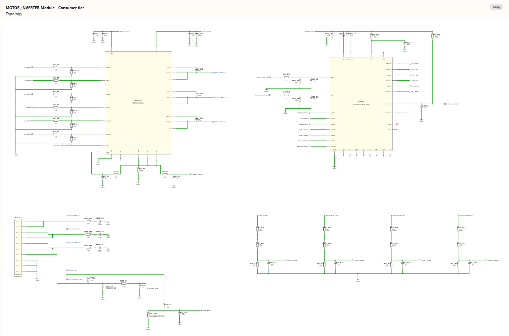
Example From a Real SpeedUp Motor-Inverter Project
The SpeedUp portable high-speed hair-dryer circuit project contains a three-phase motor-inverter sheet with candidate 51 Ω and 100 pF series networks from each phase node to power ground. The generated drawing is a useful review example because it makes the intended damping parts and their reference node visible.

Before using those values, an engineer must confirm whether the problem is differential phase ringing or common-mode current, whether power ground is the right high-frequency reference, and whether phase-to-ground capacitors create unacceptable bearing, cable, touch-current, or EMI behavior. The final values require the actual MOSFET or integrated inverter, bus voltage, gate drive, motor, cable, enclosure, layout, and measured waveforms. For a mains-powered appliance, isolation, fault protection, fire risk, accessible parts, EMC, thermal limits, and regulatory requirements also need specialist review.
How to Tune and Validate the Snubber on Hardware
- Capture a repeatable unsnubbed baseline at minimum and maximum input voltage, representative loads, startup, shutdown, and relevant fault or regeneration states.
- Fit the calculated starting R and C values with the network physically located in its intended production position.
- Measure peak voltage, ring frequency, number of visible cycles, switching transition time, gate waveform, current, and any false turn-on.
- Sweep nearby capacitor values while checking resistor temperature and switching loss. More capacitance is not automatically better.
- Sweep the resistor around the calculated value to find adequate damping without excessive peak or average power.
- Repeat with component tolerances, device variants, hot and cold conditions, cable or motor options, and maximum expected load.
- Run conducted and radiated EMI tests. A cleaner oscilloscope trace at one node does not guarantee lower emissions elsewhere.
- Measure the snubber resistor and nearby capacitor temperature in the final enclosure and confirm repetitive pulse and lifetime margins.
- Record the waveform, probe setup, values, operating point, and acceptance limits in the design-review package.
Common Snubber Circuit Mistakes
- Copying 100 pF and 100 Ω—or any other familiar pair—without measuring the real resonance.
- Measuring with a long oscilloscope ground lead and designing a snubber for probe-induced ringing.
- Connecting an earth-grounded oscilloscope clip to a high-side or mains-referenced node.
- Placing the network several centimeters from the switching device because the schematic net name is the same.
- Using signal ground as a convenient endpoint without tracing the high-frequency return current.
- Checking only nominal input and load while the worst overshoot occurs at another operating corner.
- Ignoring resistor pulse energy, capacitor voltage bias, dielectric loss, ESL, and repetitive current.
- Reducing overshoot but accepting excessive snubber temperature, switching loss, or common-mode EMI.
- Treating an RC snubber as a replacement for a flyback diode, RCD clamp, TVS, correct gate drive, or low-inductance layout.
Snubber Circuit Schematic Review Checklist
| Review question | Evidence required |
|---|---|
| What transient is being controlled? | Annotated waveform with operating condition, measurement points, probe, peak, frequency, and decay |
| Why is RC the right topology? | Comparison with layout correction, diode path, RCD clamp, TVS, gate damping, and device-rating margin |
| How were R and C chosen? | Frequency-shift calculation or topology-specific energy model plus bench-tuning record |
| Are component ratings sufficient? | Voltage, pulse, average power, current, temperature, dielectric, lifetime, and safety qualification |
| Is the reference node correct? | High-frequency loop sketch and review of common-mode, isolation, chassis, and sensing impacts |
| Can the PCB implement it? | Placement constraint, short loop, spacing, thermal copper, DNP options, and safe test access |
| Was it verified at the corners? | Waveforms, temperatures, efficiency, and EMI across voltage, load, temperature, tolerances, and variants |
How SpeedUp Fits
SpeedUp can turn a product requirement into a structured KiCad schematic draft with named switching nodes, candidate protection and damping networks, MOSFET or driver sheets, test points, power domains, and explicit design notes. That makes the transient-control intent visible enough for an engineer to review and measure instead of discovering an undocumented network after PCB layout.
The generated result is a first engineering draft, not a production-ready snubber design. Engineers still verify the topology, isolate hazardous measurements, characterize the real parasitics, calculate and tune values, select pulse-rated parts, constrain PCB placement, test EMI and thermal behavior, and complete sourcing, safety, compliance, and manufacturing work. Use the AI-generated KiCad schematic review guide for the complete pre-layout process.
FAQ
What is the purpose of a snubber circuit?
A snubber changes the transient response of a switching circuit. Depending on the topology, it can damp ringing, reduce voltage overshoot, limit contact arcing, absorb leakage-inductance energy, reduce EMI, or protect a semiconductor from repetitive stress.
How do I calculate an RC snubber?
For a measured LC ring, record the original frequency, add a known parallel test capacitor, and record the shifted frequency. Use the frequency ratio to estimate the effective parasitic capacitance and inductance, then start around three times the parasitic capacitance and a resistance equal to the square root of L divided by C. Tune and verify on the real board.
Where should an RC snubber be placed?
Place it directly across the two nodes participating in the measured resonance, with the smallest practical loop area. For a MOSFET drain-to-source network, connect close to the device power terminals. Long traces add inductance and reduce high-frequency damping.
What happens if the snubber capacitor is too large?
A larger capacitor can reduce overshoot, but it increases charge/discharge current, resistor dissipation, switching loss, and possibly common-mode current. It can also create a new resonance with the snubber path inductance. Verify efficiency, temperature, EMI, and device stress.
Is a flyback diode the same as a snubber?
Not usually. A flyback diode provides a path for inductive current when a DC load switch opens. A series RC snubber dissipates energy to damp an oscillatory transient. Some designers use “snubber” broadly for several clamp networks, so identify the actual topology rather than relying on the name.
Can a snubber replace good PCB layout?
No. Reducing the switching-loop and gate-loop inductance is normally the first action. A snubber controls the residual resonance and must itself be placed in a very low-inductance loop. Poor placement can make a correctly calculated network ineffective.
Start Your Switching Circuit Project
Turn your switching-power requirements into a schematic draft that can be measured and refined.
Use SpeedUp to turn the product requirements into structured schematic sheets and an editable KiCad first draft for engineering review. Create a free account to begin.
Comments
No comments yet.
Leave a Reply