
Quick Answer
A solder jumper is a small PCB configuration option made from pads that can be bridged with solder or cut open later. In a KiCad schematic, you should add a solder jumper only when the board needs a simple hardware-selectable option, such as boot mode, address selection, power source selection, feature enable/disable, measurement isolation, or a prototype fallback.
Do not add solder jumpers everywhere. They add layout decisions, assembly ambiguity, documentation burden, and possible reliability risk if the state is unclear. Before layout, review whether the option should be a solder jumper, a 0-ohm resistor, a DNP part, a pin header, a switch, a test point, or just firmware configuration.
For AI-generated KiCad schematics, the right workflow is: inspect the generated architecture, find the nets that may need configurable behavior, decide which options really need hardware control, and document the default state before routing the PCB.
Why Solder Jumpers Matter in AI-Generated Schematics
AI-generated schematics can produce a clean first draft, but they do not always know which choices should stay configurable in hardware. A product prompt may say "support USB-C power and battery," "include debug access," or "allow alternate sensor addresses." Those requirements can imply configuration options, but the schematic still needs engineering judgment.
A solder jumper is useful when you want a low-cost, low-profile way to change a circuit after fabrication. It is less useful when the board needs frequent user changes, production traceability, high-current switching, safety isolation, RF tuning, or a setting that firmware can handle more safely.
The review question is not "can I add a solder jumper?" The better question is:
Will this option need to change after assembly, and is a solder bridge the safest, clearest, and easiest way to change it?
If the answer is not clear, use a more explicit configuration method or document the decision before layout.
Solder Jumper Decision Checklist
| Review area | Use a solder jumper when | Avoid a solder jumper when | Better alternative |
|---|---|---|---|
| Boot or mode selection | A rare lab-only boot strap needs a default state and occasional override | The user or factory changes the setting often | Header, button, DIP switch, or dedicated boot connector |
| I2C address selection | Two possible addresses may be needed for prototype variants | Many address combinations are expected | Resistor option matrix or firmware-configurable peripheral |
| Power source selection | A prototype needs to choose between two low-current rails or enable paths | The path carries high current, safety-critical power, or hot-plug current | Load switch, ideal diode, connector option, or 0-ohm resistor with clear rating |
| Debug access | A debug signal should be isolated or optionally connected | The debug interface is used on every board | Header, tag connector, or test pads |
| Measurement isolation | A rail, sensor, or current path may need to be disconnected for measurement | The measurement requires accuracy, calibration, or repeated factory use | Shunt resistor footprint, test point pair, or removable link |
| Feature enable | A prototype feature may be turned on/off during experiments | End users need to configure it | Firmware flag, switch, connector, or assembled BOM option |
| Assembly variant | A board has one simple factory option | The choice affects compliance, safety, or documented SKU identity | Separate BOM variant with 0-ohm or DNP placement |
| Layout workaround | A short optional bridge helps route or isolate a prototype net | The bridge hides a design uncertainty that should be solved | Fix the schematic or layout constraint instead |
Need configuration options before layout?
Describe the product variants, default states, assembly choices, test modes, field configuration, and labeling requirements. Create a free account to start a reviewable, editable KiCad first draft.
Use the table as a pre-layout filter. A solder jumper is strongest when the option is rare, low-risk, low-current, easy to label, and easy to inspect visually.
Solder Jumper vs 0-Ohm Resistor vs Header
| Option | Best for | Advantages | Tradeoffs |
|---|---|---|---|
| Solder jumper | Simple one-time or rare configuration on a compact PCB | Cheap, small, no extra component if open by default | Can be messy, hard to inspect, and unclear without labels |
| 0-ohm resistor | BOM-controlled assembly variants and production options | Pick-and-place friendly, easy to document in BOM | Requires component placement and inventory control |
| DNP resistor/capacitor option | Optional pullups, filters, dividers, or tuning networks | Clear schematic intent and assembly state | More BOM discipline needed |
| Pin header / tag connector | Repeated debug, programming, or field configuration | Easy to use and reliable for repeated changes | Uses board space and may not fit enclosure |
| DIP switch or slide switch | User-facing or frequently changed settings | Clear state and no soldering required | More cost, height, and mechanical constraints |
| Firmware setting | Behavior that can safely be controlled in software | No layout/configuration pads needed | Requires firmware support and may not work before boot |
If the setting must be visible in production records, a 0-ohm or DNP part is usually cleaner than a solder bridge. If the setting is changed frequently, a header or switch is usually better. If the setting only helps a prototype engineer once or twice, a solder jumper can be perfect.
Example From a Real SpeedUp Project
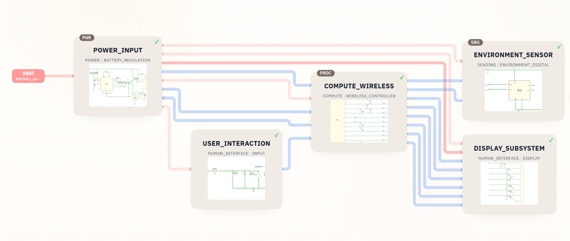
The Desktop Robot ESP32 KiCad schematic project is a useful review example because it separates the generated design into power, compute, display, sensing, and user interface sheets. That sheet structure makes it easier to see where a hardware configuration option might be useful before PCB layout.
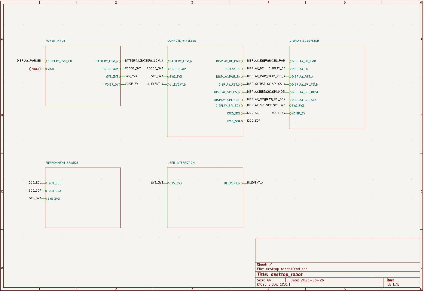
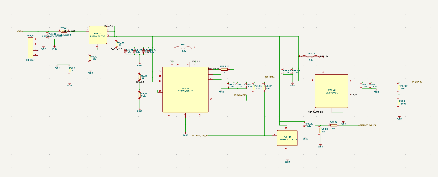
Start with power. Power paths are where solder jumpers are tempting, but also where they are easiest to misuse. A prototype might use a low-current jumper to isolate a rail, select a measurement path, or test an enable behavior. A production power path may need a real switch, protection circuit, connector option, or BOM-controlled 0-ohm resistor instead.
Then review the compute and wireless sheet. An ESP32-style design often has boot, reset, debug, programming, display, sensor, and status signals. Some of those signals may benefit from a hardware-selectable default in early prototypes. Others should stay as fixed pullups, test points, connectors, or firmware-managed behavior.
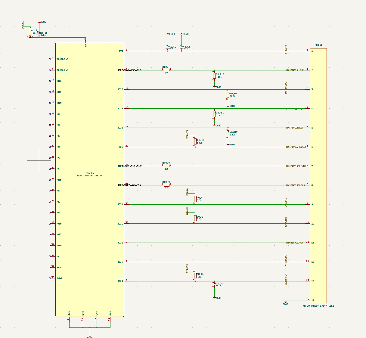
The goal is not to add solder jumpers to the screenshot after the fact. The goal is to use the generated KiCad structure as a review map: identify candidate nets, decide the safest configuration method, and document the default state before layout.
How to Add a Solder Jumper in KiCad
In KiCad, the schematic symbol and PCB footprint must describe the same manufactured default. Use a two-pad or three-pad symbol from the Jumper library, then choose an open or bridged footprint that matches how the bare PCB should arrive. Example symbol names include Jumper:SolderJumper_2_Open and Jumper:SolderJumper_2_Bridged; exact names can vary with the installed KiCad library release.
- Choose the default state first. Decide whether the unmodified PCB should be open, bridged, or connected from a common pad to one side of a three-pad option.
- Place the matching schematic symbol. Give it a clear reference such as
SJ1and a value or note that states the default behavior. - Connect and name both sides deliberately. Use net labels that make the function obvious, such as
BOOT_MODE,ADDR_SEL, orCAN_TERM_EN. - Assign a matching footprint. Select the two-pad or three-pad solder-jumper footprint whose copper is open or bridged in the same state shown by the schematic symbol.
- Run ERC and inspect pad mapping. Confirm pin numbers, net names, and the intended closed path before updating the PCB from the schematic.
- Place it for access and inspection. Keep the pads reachable by an iron, away from sensitive RF or high-voltage areas, and add a readable silkscreen reference where space permits.
- Document assembly and bring-up. Record whether the production state is open, bridged, cut, or fitted only for selected variants.
KiCad’s official Schematic Editor documentation explains how symbol properties and connected footprints carry jumper-pin information. Do not confuse a selectable solder jumper with a net tie: a net tie intentionally joins separately named nets in copper, while a solder jumper represents a configurable physical connection.
A CAN endpoint is one practical example. If termination must be optional, use a clearly documented jumper or BOM-controlled option and review the resistor network with the CAN bus termination resistor placement and testing guide; do not add a selectable 120-ohm path without defining the board’s role on the bus.
KiCad Review Flow Before Layout
Use this workflow when reviewing an AI-generated KiCad schematic:
1. List every net that may need alternate behavior: boot, reset, enable, address, debug, power select, sensor select, test isolation, and feature options. 2. For each net, write the expected default state: open, closed, pulled up, pulled down, connected to rail A, connected to rail B, or DNP. 3. Decide how often the setting will change: never, once during bring-up, sometimes in the lab, every production unit, or by the end user. 4. Choose the implementation: solder jumper, 0-ohm resistor, DNP footprint, header, switch, test point, or firmware. 5. Check current, voltage, noise, RF, safety, and signal-integrity risk before using a solder bridge. 6. Add readable schematic labels such as SJ_BOOT, SJ_ADDR, SJ_PWR_SEL, or SJ_DEBUG_EN. 7. In PCB layout, keep the pads reachable, labeled, and visually inspectable. 8. Add the default state to the bring-up notes and assembly notes.
This review should happen before PCB placement. If you wait until routing is nearly done, the jumper may land somewhere hard to reach or hard to label.
Common Mistakes
- Using a solder jumper where a 0-ohm resistor would be clearer for BOM-controlled production.
- Putting a solder jumper on a high-current path without checking current, heat, clearance, or assembly risk.
- Forgetting to document whether the default state is open or bridged.
- Using solder jumpers for settings that the user or factory must change often.
- Creating a board that boots only if someone remembers to bridge a pad manually.
- Placing the pads under a module, near a tall component, or inside an enclosure area that cannot be reached.
- Letting AI add a configurable option without asking whether the option is actually needed.
How SpeedUp Fits
SpeedUp helps generate the first KiCad schematic structure from a product description. That structure is useful because it gives engineers real sheets, nets, and subsystem boundaries to review.
For solder jumpers, SpeedUp should be part of the early review loop:
1. describe the product and constraints 2. generate the KiCad schematic project 3. inspect power, compute, sensor, debug, and interface sheets 4. mark candidate configuration nets 5. choose solder jumper, 0-ohm, DNP, header, switch, test point, or firmware 6. document defaults before PCB layout
The generated draft is not a production-ready reference design. It is a faster starting point for engineering review, including the small configuration decisions that make prototypes easier to bring up.
Related SpeedUp Projects and Guides
- Desktop Robot ESP32 KiCad Schematic Project Generated from a Prompt – the project example used in this guide.
- Battery Powered Sensor Circuit Design Checklist – a related power and bring-up checklist for compact devices.
- How to Review AI-Generated KiCad Schematics Before PCB Layout – the broader schematic review workflow.
- What to Check Before Using an AI-Generated KiCad Schematic for PCB Layout – layout readiness checks after schematic review.
- KiCad Schematic Generator: From Product Prompt to Editable KiCad Project – the prompt-to-KiCad workflow behind SpeedUp-generated projects.
FAQ
What is a solder jumper?
A solder jumper is a small pair or group of exposed PCB pads that can be connected with solder or opened by cutting a bridge. It is usually used for simple hardware configuration, prototype options, or one-time assembly choices.
When should I use a solder jumper instead of a 0-ohm resistor?
Use a solder jumper when the setting is rare, low-risk, and does not need pick-and-place assembly control. Use a 0-ohm resistor when the configuration should be documented in the BOM, assembled consistently, and inspected as a normal component.
Can I use a solder jumper for boot mode?
Yes, if boot mode only needs a rare lab override and the default state is clearly documented. If the board must be programmed repeatedly, use a proper debug connector, header, button, or fixture-friendly test access.
Should AI-generated schematics include solder jumpers automatically?
Not automatically. AI can suggest candidate configuration points, but engineers should decide whether each option belongs in hardware, firmware, BOM variants, or test access. A solder jumper is a design decision, not a decoration.
Is an EasyEDA solder jumper the same idea as a KiCad solder jumper?
The design idea is the same: exposed pads that can be bridged or opened for configuration. The exact symbol, footprint, and library workflow differ by EDA tool, so KiCad projects still need KiCad-specific symbol, footprint, clearance, labeling, and fabrication review.
Start Your Configurable Hardware Project
Make jumper choices and default states explicit in a reviewable schematic draft.
Use SpeedUp to turn the product requirements into structured schematic sheets and an editable KiCad first draft for engineering review. Create a free account to begin.
Comments
No comments yet.
Leave a Reply