
Quick Answer
A USB-C schematic is ready for PCB layout only after the port role is explicit and every signal has been reviewed against that role. Start by deciding whether the receptacle is a 5 V power sink, a USB 2.0 device, a power source, a dual-role port, or a USB Power Delivery port. Then check both CC pins, VBUS protection and current assumptions, D+ and D- routing when data is present, connector shield and ESD strategy, charger and battery boundaries, symbols, footprints, ERC results, and layout constraints.
Do not treat the USB-C connector as a drop-in replacement for Micro-USB. The connector shape does not tell a source what power role the product needs, and USB-C does not automatically mean USB PD or battery charging. A generated or copied circuit can look complete while missing a CC resistor, using the wrong connector pin mapping, assuming unavailable current, or connecting a charger without a defined system power path. Use this checklist together with the broader schematic review checklist before PCB layout.
First Decide What the USB-C Port Must Do
The correct USB-C circuit depends on the product role. Write the role beside the connector in the schematic instead of leaving the reviewer to infer it.
| Port requirement | Schematic implication | Main review risk |
|---|---|---|
| 5 V sink, no data | Two valid Rd terminations on CC1 and CC2, protected VBUS input, and a power path sized for the current the source actually advertises. | Assuming VBUS or high current will be available without a valid Type-C connection. |
| USB 2.0 device and 5 V sink | Sink detection plus the correct receptacle D+ and D- pin pairing, ESD protection, and routing to a USB PHY or bridge. | Broken cable-orientation support, long stubs, or an unprotected data pair. |
| 5 V source | Rp presentation or a CC controller, controlled VBUS switching, current limiting, discharge behavior, and fault protection. | Driving an unsafe or uncontrolled VBUS source. |
| Dual-role port | A suitable CC/role controller and a power architecture that safely changes between sink and source behavior. | Conflicting power paths or the wrong role after attachment. |
| USB PD sink or source | A USB PD controller, negotiated power contract, protected power path, firmware or configuration, and parts rated for every supported voltage and current. | Treating a USB-C receptacle as if it automatically negotiates higher voltage or power. |
Adding USB-C power, data, or charging?
Describe the port role, source or sink behavior, USB data speed, charging path, protection, connectors, and operating states. Create a free account to start a reviewable, editable KiCad first draft.
USB-C names the connector and Type-C connection behavior. USB PD is a separate protocol used when the design needs negotiated power capabilities. A battery charger is another separate function: it controls the cell charge process after the input power path has been established.
USB-C Schematic Checklist
| Review area | What to check in the schematic | Why it matters before layout |
|---|---|---|
| Port role | Label sink, source, dual-role, USB 2.0, SuperSpeed, or USB PD requirements explicitly. | The CC circuit, VBUS switch, data path, controller, and firmware all depend on the role. |
| Connector symbol | Verify every receptacle pin, duplicated VBUS/GND pins, CC1/CC2, D+/D- orientation pins, shield, and unused SuperSpeed pins. | Generic or simplified symbols can hide pins that matter electrically or mechanically. |
| CC1 and CC2 | Use the correct separate termination or controller connection on both CC pins. Confirm value, tolerance, role, and controller supply state. | The port may fail in one cable orientation or never establish a valid connection. |
| VBUS availability | Document when VBUS may appear, the allowed input range, current advertisement handling, and what happens during disconnect or role change. | An always-on or overdrawn power path can create interoperability and safety problems. |
| Protection | Select ESD, overvoltage, overcurrent, reverse-current, inrush, and short-circuit protection appropriate to the role and environment. | A connector is a direct path for cable transients, user ESD, and wiring faults. |
| USB 2.0 data | Confirm the receptacle D+ and D- pairs are combined correctly for both orientations and routed to the intended USB PHY. | Incorrect pairing or stubs can produce orientation-dependent failures or poor signal integrity. |
| Data protection and series parts | Validate low-capacitance ESD parts, any series resistors, common-mode choke assumptions, and placement notes against the PHY guidance. | Protection capacitance and routing can degrade the USB data eye. |
| Shield and ground | Define the connector shield connection, chassis or digital ground relationship, ESD return path, and mechanical tabs. | An improvised shield path can worsen ESD and EMI behavior. |
| Charger boundary | Separate Type-C attachment/current handling from battery charge current, termination, thermal limits, protection, and cell requirements. | The USB input and battery charger solve different problems. |
| System power path | Decide whether the product runs while plugged in, how the load is isolated or shared, and how the battery and system rail interact. | System load can disturb charge termination, create reverse current, or exceed the source budget. |
| Capacitance and inrush | Review VBUS capacitance, hot-plug behavior, load switch or power-path needs, and discharge requirements. | Large downstream capacitance can violate attach behavior or cause unstable hot plugging. |
| Footprint and mechanics | Match the exact receptacle MPN, pin numbering, pad layout, shell stakes, board-edge position, mating clearance, and insertion loads. | A correct symbol with the wrong footprint still produces a failed board. |
| ERC and test access | Review power-input warnings, no-connect flags, shield pins, controller states, and add useful VBUS, CC, D+/D-, battery, and ground test points. | A clean ERC does not prove correct Type-C behavior, but unexplained warnings hide real mistakes. |
1. Check CC1 and CC2 Before Anything Else
The CC pins establish attachment, orientation, and available current information. For a simple 5 V sink-only receptacle without USB PD, Texas Instruments describes using a separate 5.1 kΩ Rd resistor from each CC pin to ground in the simplest implementation. Both pins matter because a reversible cable presents its active CC connection on one side or the other. Do not replace the two terminations with one shared resistor, and do not leave one CC pin floating.
That simple circuit is not a universal answer. The TI USB Type-C and USB Power Delivery engineering guide notes that system capacitance, data requirements, and port role can require a CC controller and controlled power path. A source presents Rp rather than Rd. A dual-role or PD port needs appropriate controller behavior. The schematic should therefore state why the chosen CC implementation is valid for this exact product.
Also separate connection detection from current budgeting. A sink must not assume that every USB-C source permits the same current. If firmware or hardware cannot interpret source current advertisement, design conservatively or add a suitable controller.
2. Review VBUS, Protection, and Hot-Plug Behavior
Trace VBUS from every receptacle pin to the first protected system node. The path may need ESD protection, overvoltage protection, current limiting, reverse-current blocking, a fuse or resettable protector, a load switch, discharge control, and input capacitance selected for the actual port role. Do not scatter those functions across sheets without showing the intended sequence.
For a minimal sink, TI’s guide calls out an additional constraint: if the capacitance presented on VBUS exceeds 10 µF, the design may need to isolate the extra capacitance behind a connection-controlled power path. Treat that as a review trigger, not as permission to copy one universal load-switch circuit. Confirm the latest requirements, the chosen controller guidance, and the behavior of the complete product.
Add notes that the PCB designer can act on: place connector protection close to the entry point, keep the surge and ESD return path short, size copper for current and temperature rise, and keep sensitive analog or RF circuits away from the cable entry and switching power path.
3. Treat USB 2.0 Data as a Reversible Interface
A USB-C receptacle exposes USB 2.0 D+ and D- pins for both plug orientations. In a USB 2.0-only implementation, the corresponding receptacle pins are normally joined near the connector so the USB PHY sees one differential pair regardless of cable orientation. Verify the exact connector symbol and follow the PHY or reference-layout guidance; do not create long branches that behave like stubs.
Review the data path from connector to device: ESD array pinout and capacitance, series components if recommended, pair continuity, length mismatch, vias, reference plane, return-path interruptions, test pads, and routing through any bridge or hub. A schematic cannot prove signal integrity, so transfer the impedance, placement, and routing constraints into the PCB layout notes.
If the product needs USB 3.x, Alternate Mode, or cable e-marker support, the design becomes more complex. SuperSpeed lanes, orientation multiplexing, VCONN, retimers or redrivers, and controller configuration should not be approximated by extending a USB 2.0 circuit.
4. Separate the USB-C Input From the Battery Charger
The Type-C port establishes an input-power relationship. The charger manages a specific battery chemistry, charge voltage, current, termination, temperature, and safety boundary. Put both functions on the same review path, but do not collapse them into one block labeled “USB charging.”
For example, the MCP73831 is a linear single-cell charger with programmable current and thermal regulation. Its datasheet specifies a programmable charge-current range from 15 mA to 500 mA, but that does not mean every USB-C source, cell, package, enclosure, or PCB can safely support 500 mA. Use the current Microchip MCP73831 family datasheet, the battery documentation, source-current handling, and thermal analysis together. The related MCP73831 charger schematic checklist covers charge current, battery connector, STAT, heat, and load-sharing questions in more detail.
Decide what happens while the product is plugged in. If the system load shares the battery node, it can affect charge termination and thermal behavior. If the product must run and charge at the same time, document the power-path or load-sharing solution rather than assuming the charger IC solves it automatically.
Example From a Real SpeedUp Project
The nRF54L15 development-board KiCad project contains a generated USB-C debug sheet with a 16-pin Type-C receptacle, separate 5.1 kΩ CC terminations, a USB data ESD device, series resistors, a USB-to-UART bridge, and a debug header.

This is the right role for an AI-generated schematic: make the intended circuit concrete enough to review. It is not evidence that the interface is compliant or production-ready. An engineer still checks it against the exact connector drawing, controller and bridge documentation, current Type-C requirements, layout constraints, prototype measurements, and any applicable compliance plan.
Common USB-C Schematic Mistakes
- Adding a USB-C receptacle but omitting CC terminations or handling only one cable orientation.
- Assuming USB-C automatically provides USB PD voltage, maximum current, or battery charging.
- Using one generic connector symbol without validating hidden, duplicated, shield, or mechanical pins.
- Joining D+ and D- orientation pins with long branches or routing them without an uninterrupted return path.
- Selecting ESD protection by voltage alone and ignoring capacitance, clamping behavior, package, and placement.
- Placing large capacitance directly on VBUS without reviewing inrush and attach behavior.
- Connecting a battery charger without defining cell protection, system load sharing, charge current, or thermal limits.
- Treating a clean KiCad ERC as proof that USB-C behavior and compliance are correct.
KiCad and PCB Layout Handoff
Before layout, open the exact connector footprint and compare it with the manufacturer drawing from both the board and mating perspectives. Confirm pad numbering, shell stakes, board edge, cutouts, courtyard, connector height, insertion clearance, and whether the footprint is intended for mid-mount, top-mount, or through-hole reinforcement.
Run ERC and inspect every USB-related result manually. Power-input warnings may reveal an undefined VBUS source. Unconnected pins may be intentionally unused SuperSpeed pins or a missing CC connection. Shield pins and mounting tabs may not fit ordinary signal rules. Record the reason for every no-connect and waiver so the next reviewer can distinguish a deliberate decision from a hidden mistake.
The layout handoff should name protection placement, USB differential-pair constraints, return path, connector keepout, VBUS current and copper needs, shield strategy, test access, charger thermal copper, battery separation, and any controller configuration still owned by firmware. Schematic approval is not manufacturing approval; prototype validation, signal-integrity checks, ESD testing, thermal testing, DFM, and compliance work remain.
How SpeedUp Fits
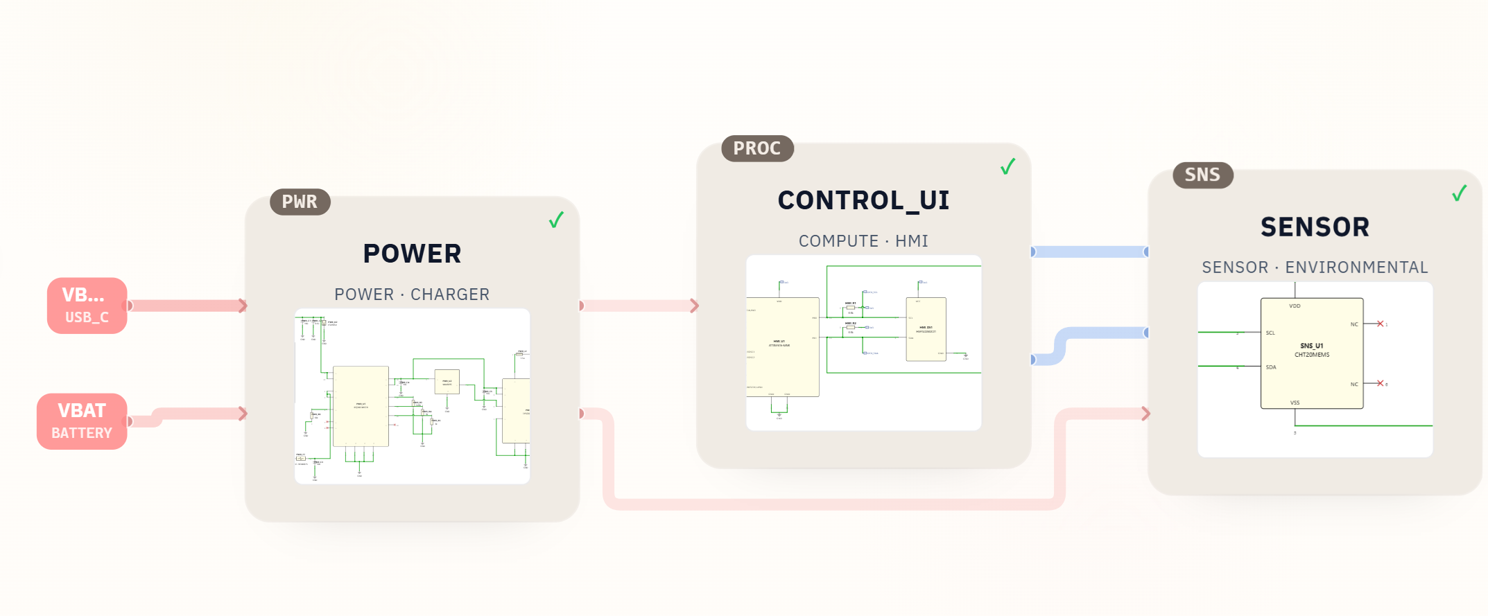
SpeedUp can turn a product requirement into a structured first engineering draft with a block diagram, schematic hierarchy, components, and editable KiCad files. For a USB-C product, a useful prompt should state the port role, data speed, input or output power, battery and charger behavior, system load while connected, protection needs, connector constraints, test points, and expected firmware ownership.
The goal is not to skip USB-C engineering. The goal is to expose the decisions earlier so an engineer can review the CC implementation, power path, data pair, protection, charger, footprints, and layout constraints before the PCB is committed.
Related SpeedUp Guides and Projects
- Temperature and humidity sensor KiCad project with USB-C charging – a battery-powered sensor example that connects USB-C input, charging, regulation, display, and sensing.
- Battery-powered sensor circuit design checklist – broader review of charging, rails, sleep current, I2C sensors, displays, and layout risks.
FAQ
Does a USB-C sink need resistors on both CC pins?
A simple 5 V sink-only receptacle normally uses a separate Rd termination on CC1 and CC2 so attachment works in either cable orientation. TI’s engineering guide shows 5.1 kΩ for this basic case. Verify the latest Type-C requirements and use a controller when the port role, current handling, capacitance, data, or PD requirements exceed the simple case.
Is USB-C the same as USB Power Delivery?
No. USB-C describes the connector and Type-C connection system. USB PD adds protocol-based power negotiation over the CC connection. A product using a USB-C connector does not automatically support higher PD voltages or power levels.
Can I connect a USB-C receptacle directly to a battery charger?
Only after the Type-C sink behavior, available current, VBUS protection, inrush, and charger input limits are correctly handled. The charger must also match the cell chemistry, charge voltage, current, thermal environment, protection, and system load behavior.
How should USB 2.0 D+ and D- be connected on a Type-C receptacle?
A USB 2.0-only receptacle implementation normally combines the matching D+ orientation pins and the matching D- orientation pins near the connector, then routes one differential pair to the USB PHY. Verify the exact connector symbol and device guidance, keep branches short, and include suitable low-capacitance protection.
Does passing KiCad ERC mean a USB-C schematic is correct?
No. ERC can catch some connectivity and pin-rule problems, but it does not validate the Type-C role, current assumptions, USB PD behavior, charger safety, connector footprint, data signal integrity, ESD performance, firmware configuration, or compliance.
Start Your USB-C Hardware Project
Turn your USB-C role and power requirements into a structured, editable KiCad first draft.
Use SpeedUp to turn the product requirements into structured schematic sheets and an editable KiCad first draft for engineering review. Create a free account to begin.
Comments
No comments yet.
Leave a Reply