
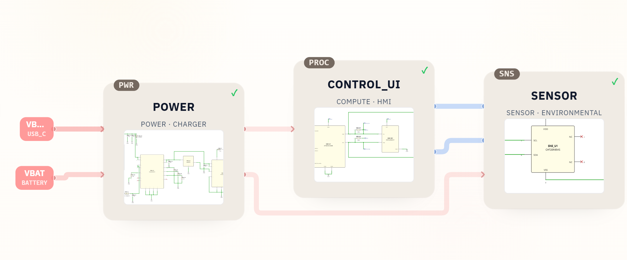
USB-C Schematic Checklist Before PCB Layout: Power, Data, and Charging
Review a USB-C schematic before PCB layout: CC resistors, VBUS, USB 2.0 data, ESD protection, charging, power paths, footprints, ERC, and release risks.
Review a USB-C schematic before PCB layout: CC resistors, VBUS, USB 2.0 data, ESD protection, charging, power paths, footprints, ERC, and release risks.
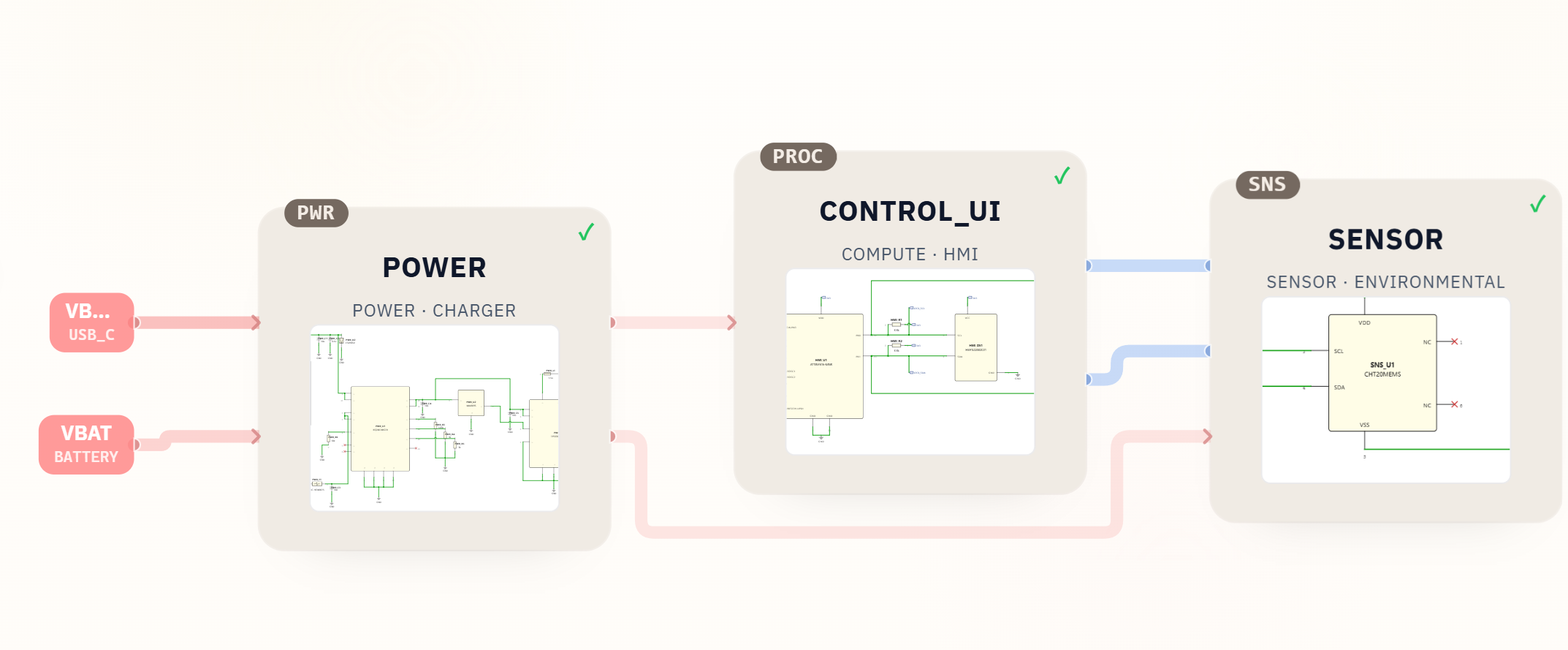
Review a BME280 KiCad schematic before PCB layout: I2C pullups, power rails, address pins, decoupling, sensor placement, airflow, thermal isolation, and BOM.
Review an SN65HVD230 CAN bus schematic before PCB layout: 3.3 V supply, CANH/CANL, termination, slope control, standby, ESD, connector, and KiCad checks.
Review an MCP73831 charger circuit before PCB layout: input power, charge current, battery connector, STAT pin, thermal limits, load sharing, and KiCad checks.
Compare AI PCB design software by workflow: product prompt to schematic, schematic and BOM generation, PCB layout automation, code-first design, and review.
Compare PCB board vs breadboard prototyping, learn when to move into a KiCad schematic, and use a review checklist with real SpeedUp examples.
Learn when to use a solder jumper in a KiCad schematic, when to choose a header or 0-ohm resistor, and how to review AI-generated designs before layout.
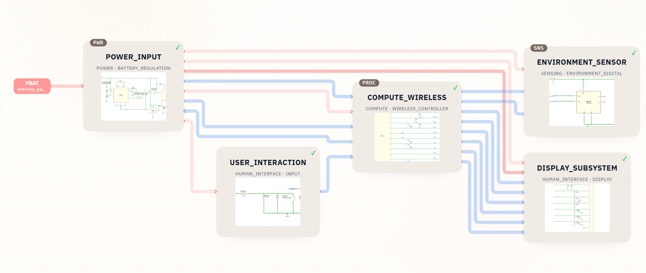
Review a generated desktop robot ESP32 KiCad schematic with power regulation, display wiring, environment sensing, BOM, and downloadable project files.
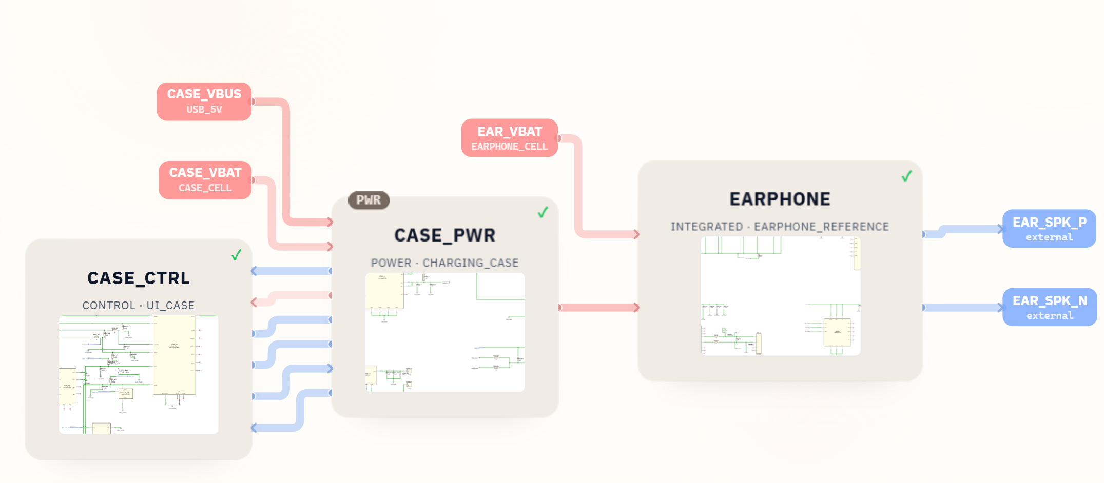
Download an editable TWS earbuds KiCad project with three schematic sheets, BOM, local libraries, and a placed but unrouted PCB file.